
User Manual
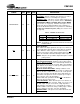
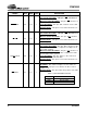
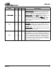
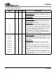
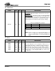
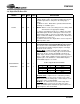
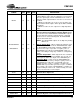
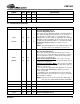
Table Of Contents
- Features
- Description
- 1. Pin Out - 144-Pin LQFP Package
- 2. Pin Out - 160-Ball FBGA Package
- 3. Pin Descriptions
- 4. operation
- 5. Power-up
- 6. Master Clock
- 7. G.772 Monitoring
- 8. Building Integrated Timing Systems (BITS) Clock Mode
- 9. Transmitter
- 10. Receiver
- 11. Jitter Attenuator
- 12. Operational Summary
- 13. Host Mode
- 14. Register Descriptions
- 14.1 Revision/IDcode Register (00h)
- 14.2 Analog Loopback Register (01h)
- 14.3 Remote Loopback Register (02h)
- 14.4 TAOS Enable Register (03h)
- 14.5 LOS Status Register (04h)
- 14.6 DFM Status Register (05h)
- 14.7 LOS Interrupt Enable Register (06h)
- 14.8 DFM Interrupt Enable Register (07h)
- 14.9 LOS Interrupt Status Register (08h)
- 14.10 DFM Interrupt Status Register (09h)
- 14.11 Software Reset Register (0Ah)
- 14.12 Performance Monitor Register (0Bh)
- 14.13 Digital Loopback Reset Register (0Ch)
- 14.14 LOS/AIS Mode Enable Register (0Dh)
- 14.15 Automatic TAOS Register (0Eh)
- 14.16 Global Control Register (0Fh)
- 14.17 Line Length Channel ID Register (10h)
- 14.18 Line Length Data Register (11h)
- 14.19 Output Disable Register (12h)
- 14.20 AIS Status Register (13h)
- 14.21 AIS Interrupt Enable Register (14h)
- 14.22 AIS Interrupt Status Register (15h)
- 14.23 AWG Broadcast Register (16h)
- 14.24 AWG Phase Address Register (17h)
- 14.25 AWG Phase Data Register (18h)
- 14.26 AWG Enable Register (19h)
- 14.27 Reserved Register (1Ah)
- 14.28 Reserved Register (1Bh)
- 14.29 Reserved Register (1Ch)
- 14.30 Reserved Register (1Dh)
- 14.31 Bits Clock Enable Register (1Eh)
- 14.32 Reserved Register (1Fh)
- 14.33 Status Registers
- 15. Arbitrary Waveform Generator
- 16. JTAG Support
- 17. Boundary Scan Register (BSR)
- 18. Applications
- 19. Characteristics and specifications
- 19.1 Absolute Maximum Ratings
- 19.2 Recommended Operating Conditions
- 19.3 Digital Characteristics
- 19.4 Transmitter Analog Characteristics
- 19.5 Receiver Analog Characteristics
- 19.6 Jitter Attenuator Characteristics
- 19.7 Master Clock Switching Characteristics
- 19.8 Transmit Switching Characteristics
- 19.9 Receive Switching Characteristics
- 19.10 Switching Characteristics - Serial Port
- 19.11 Switching Characteristics - Parallel Port (Multiplexed Mode)
- 19.12 Switching Characteristics- Parallel Port (Non-Multiplexed Mode)
- 19.13 Switching Characteristics - JTAG
- 20. Compliant Recommendations and specifications
- 21. 160-Ball FBGA package dimensions
- 22. 144-Pin LQFP Package dimensions
CS61880
18 DS450PP3
RCLK2 78 M14 O Receive Clock Output Port 2
RPOS2/RDATA2 77 M13 O Receive Positive Pulse/ Receive Data Output Port 2
RNEG2/BPV2 76 M12 O Receive Negative Pulse/Bipolar Violation Output Port 2
TCLK3 74 N14 I Transmit Clock Input Port 3
TPOS3/TDATA3 73 N13 I Transmit Positive Pulse/Transmit Data Input Port 3
TNEG3/UBS3 72 N12 I Transmit Negative Pulse/Unipolar-Bipolar Select Port 3
RCLK3 71 P14 O Receive Clock Output Port 3
RPOS3/RDATA3 70 P13 O Receive Positive Pulse/ Receive Data Output Port 3
RNEG3/BPV3 69 P12 O Receive Negative Pulse/Bipolar Violation Output Port 3
TCLK4 107 B14 I Transmit Clock Input Port 4
TPOS4/TDATA4 108 B13 I Transmit Positive Pulse/Transmit Data Input Port 4
TNEG4/UBS4 109 B12 I Transmit Negative Pulse/Unipolar-Bipolar Select Port 4
RCLK4 110 A14 O Receive Clock Output Port 4
RPOS4/RDATA4 111 A13 O Receive Positive Pulse/ Receive Data Output Port 4
RNEG4/BPV4 112 A12 O Receive Negative Pulse/Bipolar Violation Output Port 4
TCLK5 100 D14 I Transmit Clock Input Port 5
TPOS5/TDATA5 101 D13 I Transmit Positive Pulse/Transmit Data Input Port 5
TNEG5/UBS5 102 D12 I Transmit Negative Pulse/Unipolar-Bipolar Select Port 5
RCLK5 103 C14 O Receive Clock Output Port 5
RPOS5/RDATA5 104 C13 O Receive Positive Pulse/ Receive Data Output Port 5
RNEG5/BPV5 105 C12 O Receive Negative Pulse/Bipolar Violation Output Port 5
TCLK6 9 D1 I Transmit Clock Input Port 6
TPOS6/TDATA6 8 D2 I Transmit Positive Pulse/Transmit Data Input Port 6
TNEG6/UBS6 7 D3 I Transmit Negative Pulse/Unipolar-Bipolar Select Port 6
RCLK6 6 C1 O Receive Clock Output Port 6
RPOS6/RDATA6 5 C2 O Receive Positive Pulse/ Receive Data Output Port 6
RNEG6/BPV6 4 C3 O Receive Negative Pulse/Bipolar Violation Output Port 6
TCLK7 2 B1 I Transmit Clock Input Port 7
TPOS7/TDATA7 1 B2 I Transmit Positive Pulse/Transmit Data Input Port 7
TNEG7/UBS7 144 B3 I Transmit Negative Pulse/Unipolar-Bipolar Select Port 7
SYMBOL LQFP FBGA TYPE DESCRIPTION