
User Manual
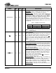
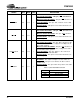
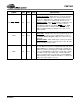
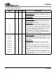
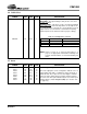
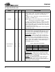
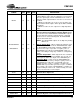
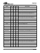
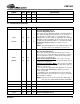
Table Of Contents
- Features
- Description
- 1. Pin Out - 144-Pin LQFP Package
- 2. Pin Out - 160-Ball FBGA Package
- 3. Pin Descriptions
- 4. operation
- 5. Power-up
- 6. Master Clock
- 7. G.772 Monitoring
- 8. Building Integrated Timing Systems (BITS) Clock Mode
- 9. Transmitter
- 10. Receiver
- 11. Jitter Attenuator
- 12. Operational Summary
- 13. Host Mode
- 14. Register Descriptions
- 14.1 Revision/IDcode Register (00h)
- 14.2 Analog Loopback Register (01h)
- 14.3 Remote Loopback Register (02h)
- 14.4 TAOS Enable Register (03h)
- 14.5 LOS Status Register (04h)
- 14.6 DFM Status Register (05h)
- 14.7 LOS Interrupt Enable Register (06h)
- 14.8 DFM Interrupt Enable Register (07h)
- 14.9 LOS Interrupt Status Register (08h)
- 14.10 DFM Interrupt Status Register (09h)
- 14.11 Software Reset Register (0Ah)
- 14.12 Performance Monitor Register (0Bh)
- 14.13 Digital Loopback Reset Register (0Ch)
- 14.14 LOS/AIS Mode Enable Register (0Dh)
- 14.15 Automatic TAOS Register (0Eh)
- 14.16 Global Control Register (0Fh)
- 14.17 Line Length Channel ID Register (10h)
- 14.18 Line Length Data Register (11h)
- 14.19 Output Disable Register (12h)
- 14.20 AIS Status Register (13h)
- 14.21 AIS Interrupt Enable Register (14h)
- 14.22 AIS Interrupt Status Register (15h)
- 14.23 AWG Broadcast Register (16h)
- 14.24 AWG Phase Address Register (17h)
- 14.25 AWG Phase Data Register (18h)
- 14.26 AWG Enable Register (19h)
- 14.27 Reserved Register (1Ah)
- 14.28 Reserved Register (1Bh)
- 14.29 Reserved Register (1Ch)
- 14.30 Reserved Register (1Dh)
- 14.31 Bits Clock Enable Register (1Eh)
- 14.32 Reserved Register (1Fh)
- 14.33 Status Registers
- 15. Arbitrary Waveform Generator
- 16. JTAG Support
- 17. Boundary Scan Register (BSR)
- 18. Applications
- 19. Characteristics and specifications
- 19.1 Absolute Maximum Ratings
- 19.2 Recommended Operating Conditions
- 19.3 Digital Characteristics
- 19.4 Transmitter Analog Characteristics
- 19.5 Receiver Analog Characteristics
- 19.6 Jitter Attenuator Characteristics
- 19.7 Master Clock Switching Characteristics
- 19.8 Transmit Switching Characteristics
- 19.9 Receive Switching Characteristics
- 19.10 Switching Characteristics - Serial Port
- 19.11 Switching Characteristics - Parallel Port (Multiplexed Mode)
- 19.12 Switching Characteristics- Parallel Port (Non-Multiplexed Mode)
- 19.13 Switching Characteristics - JTAG
- 20. Compliant Recommendations and specifications
- 21. 160-Ball FBGA package dimensions
- 22. 144-Pin LQFP Package dimensions
CS61880
DS450PP3 17
RCLK0 39 P1 O
Receive Clock Output Port 0
- When MCLK is active, this pin outputs the recovered clock
from the signal input on RTIP and RRING. In the event of
LOS, the RCLK output transitions from the recovered clock
to MCLK.
- If MCLK is held “High”, the clock recovery circuitry is dis-
abled and the RCLK output is driven by the XOR of RNEG
and RPOS.
- If MCLK is held “Low”, this output is in a high-impedance
state.
RPOS0/RDATA0
RNEG0/BPV0
40
41
P2
P3
O
O
Receive Positive Pulse/ Receive Data Output Port 0
Receive Negative Pulse/Bipolar Violation Output Port 0
The function of the RPOS/RDATA and RNEG/BPV outputs
are determined by whether Unipolar, Bipolar, or RZ input
mode has been selected. During LOS, the RPOS/RNEG
outputs will remain active.
NOTE: The RPOS/RNEG outputs can be High-Z by holding
MCLK Low.
Bipolar Output Mode
- When configured for Bipolar opera-
tion, NRZ Data is recovered from RTIP/RRING and output
on RPOS/RNEG. A high signal on RPOS or RNEG corre-
spond to the receipt of a positive or negative pulse on
RTIP/RRING respectively. The RPOS/RNEG outputs are
valid on the falling or rising edge of RCLK as configured by
CLKE.
Unipolar Output Mode
- When unipolar mode is activated,
the recovered data is output on RDATA. The decoder sig-
nals bipolar violations are output on the RNEG/BPV pin.
RZ Output Mode
- In this mode, the RPOS/RNEG pins
output RZ data recovered by slicing the signal present on
RTIP/RRING. A positive pulse on RTIP with respect to
RRING generates a logic 1 on RPOS; a positive pulse on
RRING with respect to RTIP generates a logic 1 on RNEG.
The polarity of the output on RPOS/RNEG is selectable us-
ing the CLKE pin. In this mode, external circuitry is used to
recover clock from the received signal.
TCLK1 29 L1 I Transmit Clock Input Port 1
TPOS1/TDATA1 30 L2 I Transmit Positive Pulse/Transmit Data Input Port 1
TNEG1/UBS1 31 L3 I Transmit Negative Pulse/Unipolar-Bipolar Select Port 1
RCLK1 32 M1 O Receive Clock Output Port 1
RPOS1/RDATA1 33 M2 O Receive Positive Pulse/ Receive Data Output Port 1
RNEG1/BPV1 34 M3 O Receive Negative Pulse/Bipolar Violation Output Port 1
TCLK2 81 L14 I Transmit Clock Input Port 2
TPOS2/TDATA2 80 L13 I Transmit Positive Pulse/Transmit Data Input Port 2
TNEG2/UBS2 79 L12 I Transmit Negative Pulse/Unipolar-Bipolar Select Port 2
SYMBOL LQFP FBGA TYPE DESCRIPTION