
User Manual
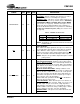
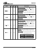
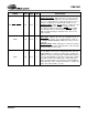
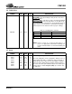
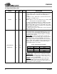
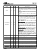
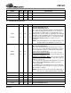
Table Of Contents
- Features
- Description
- 1. Pin Out - 144-Pin LQFP Package
- 2. Pin Out - 160-Ball FBGA Package
- 3. Pin Descriptions
- 4. operation
- 5. Power-up
- 6. Master Clock
- 7. G.772 Monitoring
- 8. Building Integrated Timing Systems (BITS) Clock Mode
- 9. Transmitter
- 10. Receiver
- 11. Jitter Attenuator
- 12. Operational Summary
- 13. Host Mode
- 14. Register Descriptions
- 14.1 Revision/IDcode Register (00h)
- 14.2 Analog Loopback Register (01h)
- 14.3 Remote Loopback Register (02h)
- 14.4 TAOS Enable Register (03h)
- 14.5 LOS Status Register (04h)
- 14.6 DFM Status Register (05h)
- 14.7 LOS Interrupt Enable Register (06h)
- 14.8 DFM Interrupt Enable Register (07h)
- 14.9 LOS Interrupt Status Register (08h)
- 14.10 DFM Interrupt Status Register (09h)
- 14.11 Software Reset Register (0Ah)
- 14.12 Performance Monitor Register (0Bh)
- 14.13 Digital Loopback Reset Register (0Ch)
- 14.14 LOS/AIS Mode Enable Register (0Dh)
- 14.15 Automatic TAOS Register (0Eh)
- 14.16 Global Control Register (0Fh)
- 14.17 Line Length Channel ID Register (10h)
- 14.18 Line Length Data Register (11h)
- 14.19 Output Disable Register (12h)
- 14.20 AIS Status Register (13h)
- 14.21 AIS Interrupt Enable Register (14h)
- 14.22 AIS Interrupt Status Register (15h)
- 14.23 AWG Broadcast Register (16h)
- 14.24 AWG Phase Address Register (17h)
- 14.25 AWG Phase Data Register (18h)
- 14.26 AWG Enable Register (19h)
- 14.27 Reserved Register (1Ah)
- 14.28 Reserved Register (1Bh)
- 14.29 Reserved Register (1Ch)
- 14.30 Reserved Register (1Dh)
- 14.31 Bits Clock Enable Register (1Eh)
- 14.32 Reserved Register (1Fh)
- 14.33 Status Registers
- 15. Arbitrary Waveform Generator
- 16. JTAG Support
- 17. Boundary Scan Register (BSR)
- 18. Applications
- 19. Characteristics and specifications
- 19.1 Absolute Maximum Ratings
- 19.2 Recommended Operating Conditions
- 19.3 Digital Characteristics
- 19.4 Transmitter Analog Characteristics
- 19.5 Receiver Analog Characteristics
- 19.6 Jitter Attenuator Characteristics
- 19.7 Master Clock Switching Characteristics
- 19.8 Transmit Switching Characteristics
- 19.9 Receive Switching Characteristics
- 19.10 Switching Characteristics - Serial Port
- 19.11 Switching Characteristics - Parallel Port (Multiplexed Mode)
- 19.12 Switching Characteristics- Parallel Port (Non-Multiplexed Mode)
- 19.13 Switching Characteristics - JTAG
- 20. Compliant Recommendations and specifications
- 21. 160-Ball FBGA package dimensions
- 22. 144-Pin LQFP Package dimensions
CS61880
16 DS450PP3
3.6 Digital Rx/Tx Data I/O
SYMBOL LQFP FBGA TYPE DESCRIPTION
TCLK0 36 N1 I
Transmit Clock Input Port 0
- When TCLK is active, the TPOS and TNEG pins function
as NRZ inputs that are sampled on the falling edge of
TCLK.
- If MCLK is active, TAOS will be generated when TCLK is
held High for 16 MCLK cycles.
NOTE: MCLK is used as the timing reference during TAOS
and must have the appropriate stability.
- If TCLK is held High in the absence of MCLK, the TPOS
and TNEG inputs function as RZ inputs. In this mode, the
transmit pulse width is set by the pulse-width of the signal
input on TPOS and TNEG. To enter this mode, TCLK must
be held high for at least 12 µs.
- If TCLK is held Low, the output drivers enter a low-power,
high impedance state.
TPOS0/TDATA0
TNEG0/UBS
37
38
N2
N3
I
I
Transmit Positive Pulse/Transmit Data Input Port 0
Transmit Negative Pulse/Unipolar-Bipolar Select Port 0
The function of the TPOS/TDATA and TNEG/UBS inputs
are determined by whether Unipolar, Bipolar or RZ input
mode has been selected.
Bipolar Mode
- In this mode, NRZ data on TPOS and
TNEG are sampled on the falling edge of TCLK and trans-
mitted onto the line at TTIP and TRING respectively. A
“High” input on TPOS results in transmission of a positive
pulse; a “High” input on TNEG results in a transmission of a
negative pulse. The translation of TPOS/TNEG inputs to
TTIP/TRING outputs is as follows:
Unipolar mode
- Unipolar mode is activated by holding
TNEG/UBS “High” for more than 16 TCLK cycles, when
MCLK is present. The falling edge of TCLK samples a uni-
polar data steam on TPOS/TDATA.
RZ Mode
- To activate RZ mode tie TCLK “High” in the
absence of MCLK. In this mode, the duty cycle of the
TPOS and TNEG inputs determine the pulse width of the
output signal on TTIP and TRING.
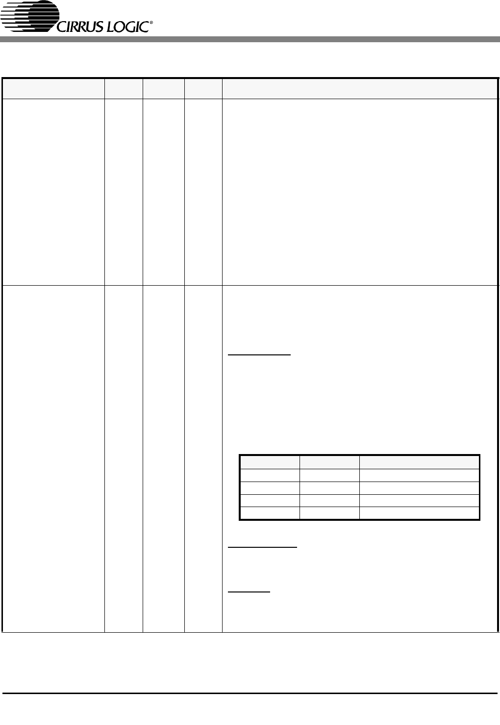
Table 5. Bipolar Mode Translations
TPOS TNEG OUTPUT
0 0 Space
1 0 Positive Mark
0 1 Negative Mark
1 1 Space