
User Manual
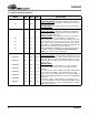
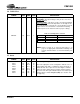
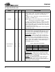
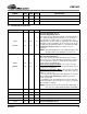
Table Of Contents
- Features
- Description
- 1. Pin Out - 144-Pin LQFP Package
- 2. Pin Out - 160-Ball FBGA Package
- 3. Pin Descriptions
- 4. operation
- 5. Power-up
- 6. Master Clock
- 7. G.772 Monitoring
- 8. Building Integrated Timing Systems (BITS) Clock Mode
- 9. Transmitter
- 10. Receiver
- 11. Jitter Attenuator
- 12. Operational Summary
- 13. Host Mode
- 14. Register Descriptions
- 14.1 Revision/IDcode Register (00h)
- 14.2 Analog Loopback Register (01h)
- 14.3 Remote Loopback Register (02h)
- 14.4 TAOS Enable Register (03h)
- 14.5 LOS Status Register (04h)
- 14.6 DFM Status Register (05h)
- 14.7 LOS Interrupt Enable Register (06h)
- 14.8 DFM Interrupt Enable Register (07h)
- 14.9 LOS Interrupt Status Register (08h)
- 14.10 DFM Interrupt Status Register (09h)
- 14.11 Software Reset Register (0Ah)
- 14.12 Performance Monitor Register (0Bh)
- 14.13 Digital Loopback Reset Register (0Ch)
- 14.14 LOS/AIS Mode Enable Register (0Dh)
- 14.15 Automatic TAOS Register (0Eh)
- 14.16 Global Control Register (0Fh)
- 14.17 Line Length Channel ID Register (10h)
- 14.18 Line Length Data Register (11h)
- 14.19 Output Disable Register (12h)
- 14.20 AIS Status Register (13h)
- 14.21 AIS Interrupt Enable Register (14h)
- 14.22 AIS Interrupt Status Register (15h)
- 14.23 AWG Broadcast Register (16h)
- 14.24 AWG Phase Address Register (17h)
- 14.25 AWG Phase Data Register (18h)
- 14.26 AWG Enable Register (19h)
- 14.27 Reserved Register (1Ah)
- 14.28 Reserved Register (1Bh)
- 14.29 Reserved Register (1Ch)
- 14.30 Reserved Register (1Dh)
- 14.31 Bits Clock Enable Register (1Eh)
- 14.32 Reserved Register (1Fh)
- 14.33 Status Registers
- 15. Arbitrary Waveform Generator
- 16. JTAG Support
- 17. Boundary Scan Register (BSR)
- 18. Applications
- 19. Characteristics and specifications
- 19.1 Absolute Maximum Ratings
- 19.2 Recommended Operating Conditions
- 19.3 Digital Characteristics
- 19.4 Transmitter Analog Characteristics
- 19.5 Receiver Analog Characteristics
- 19.6 Jitter Attenuator Characteristics
- 19.7 Master Clock Switching Characteristics
- 19.8 Transmit Switching Characteristics
- 19.9 Receive Switching Characteristics
- 19.10 Switching Characteristics - Serial Port
- 19.11 Switching Characteristics - Parallel Port (Multiplexed Mode)
- 19.12 Switching Characteristics- Parallel Port (Non-Multiplexed Mode)
- 19.13 Switching Characteristics - JTAG
- 20. Compliant Recommendations and specifications
- 21. 160-Ball FBGA package dimensions
- 22. 144-Pin LQFP Package dimensions
CS61880
12 DS450PP3
WR/DS/SDI 84 J14 I
Write Enable/Data Strobe/Serial Data
Intel Parallel Host Mode
- This pin, “WR”, functions as
a write enable.
Motorola Parallel Host Mode
- This pin, “DS“, functions as
a data strobe input.
Serial Host Mode
- This pin, “SDI”, functions as the serial
data input.
Hardware Mode
- This pin is not used and should be con-
nected to ground.
RD
/RW 85 J13 I
Read Enable/Read/Write
Intel Parallel Host Mode
- This pin, “RD”, functions as a
read enable.
Motorola Parallel Host Mode
- This pin, “R/W”, functions
as the read/write input signal.
Hardware Mode
- This pin is not used and should be con-
nected to ground.
ALE/AS
/SCLK 86 J12 I
Address Latch Enable/Address Strobe/Serial Clock
Intel Parallel Host Mode
- This pin, “ALE”, functions as the
Address Latch Enable when configured for multiplexed ad-
dress/data operation.
Motorola Parallel Host Mode
- This pin, “AS”, functions as
the active “low” address strobe when configured for multi-
plexed address/data operation.
Serial Host Mode
- This pin, “SCLK”, is the serial clock
used for data I/O on SDI and SDO.
Hardware Mode
- This pin is not used and should be con-
nected to ground.
CS
/JASEL 87 J11 I
Chip Select Input/Jitter Attenuator Select
Host Mode
- This active low input is used to enable ac-
cesses to the microprocessor interface in either serial or
parallel mode.
Hardware Mode
- This pin controls the position of the Jitter
Attenuator.
SYMBOL LQFP FBGA TYPE DESCRIPTION
Table 3. Jitter Attenuation Selection
Pin State Jitter Attenuation Position
LOW Transmit Path
HIGH Receive Path
OPEN Disabled