
User Manual
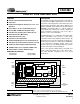
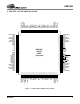
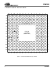
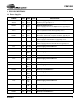
Table Of Contents
- Features
- Description
- 1. Pin Out - 144-Pin LQFP Package
- 2. Pin Out - 160-Ball FBGA Package
- 3. Pin Descriptions
- 4. operation
- 5. Power-up
- 6. Master Clock
- 7. G.772 Monitoring
- 8. Building Integrated Timing Systems (BITS) Clock Mode
- 9. Transmitter
- 10. Receiver
- 11. Jitter Attenuator
- 12. Operational Summary
- 13. Host Mode
- 14. Register Descriptions
- 14.1 Revision/IDcode Register (00h)
- 14.2 Analog Loopback Register (01h)
- 14.3 Remote Loopback Register (02h)
- 14.4 TAOS Enable Register (03h)
- 14.5 LOS Status Register (04h)
- 14.6 DFM Status Register (05h)
- 14.7 LOS Interrupt Enable Register (06h)
- 14.8 DFM Interrupt Enable Register (07h)
- 14.9 LOS Interrupt Status Register (08h)
- 14.10 DFM Interrupt Status Register (09h)
- 14.11 Software Reset Register (0Ah)
- 14.12 Performance Monitor Register (0Bh)
- 14.13 Digital Loopback Reset Register (0Ch)
- 14.14 LOS/AIS Mode Enable Register (0Dh)
- 14.15 Automatic TAOS Register (0Eh)
- 14.16 Global Control Register (0Fh)
- 14.17 Line Length Channel ID Register (10h)
- 14.18 Line Length Data Register (11h)
- 14.19 Output Disable Register (12h)
- 14.20 AIS Status Register (13h)
- 14.21 AIS Interrupt Enable Register (14h)
- 14.22 AIS Interrupt Status Register (15h)
- 14.23 AWG Broadcast Register (16h)
- 14.24 AWG Phase Address Register (17h)
- 14.25 AWG Phase Data Register (18h)
- 14.26 AWG Enable Register (19h)
- 14.27 Reserved Register (1Ah)
- 14.28 Reserved Register (1Bh)
- 14.29 Reserved Register (1Ch)
- 14.30 Reserved Register (1Dh)
- 14.31 Bits Clock Enable Register (1Eh)
- 14.32 Reserved Register (1Fh)
- 14.33 Status Registers
- 15. Arbitrary Waveform Generator
- 16. JTAG Support
- 17. Boundary Scan Register (BSR)
- 18. Applications
- 19. Characteristics and specifications
- 19.1 Absolute Maximum Ratings
- 19.2 Recommended Operating Conditions
- 19.3 Digital Characteristics
- 19.4 Transmitter Analog Characteristics
- 19.5 Receiver Analog Characteristics
- 19.6 Jitter Attenuator Characteristics
- 19.7 Master Clock Switching Characteristics
- 19.8 Transmit Switching Characteristics
- 19.9 Receive Switching Characteristics
- 19.10 Switching Characteristics - Serial Port
- 19.11 Switching Characteristics - Parallel Port (Multiplexed Mode)
- 19.12 Switching Characteristics- Parallel Port (Non-Multiplexed Mode)
- 19.13 Switching Characteristics - JTAG
- 20. Compliant Recommendations and specifications
- 21. 160-Ball FBGA package dimensions
- 22. 144-Pin LQFP Package dimensions
CS61880
10 DS450PP3
3.2 Control
SYMBOL LQFP FBGA TYPE DESCRIPTION
MCLK 10 E1 I
Master Clock Input
This pin is a free running reference clock that should be
2.048 MHz. This timing reference is used as follows:
- Timing reference for the clock recovery and jitter attenua-
tion circuitry.
- RCLK reference during Loss of Signal (LOS) conditions
- Transmit clock reference during Transmit all Ones (TAOS)
condition
- Wait state timing for microprocessor interface
- When this pin is held “High”, the PLL clock recovery cir-
cuit is disabled. In this mode, the CS61880 receivers
function as simple data slicers.
- When this pin is held “Low”, the receiver paths are pow-
ered down and the output pins RCLK, RPOS, and RNEG
are High-Z.
MODE 11 E2 I
Mode Select
This pin is used to select whether the CS61880 operates in
Serial host, Parallel host or Hardware mode.
Host Mode
- The CS61880 is controlled through either a
serial or a parallel microprocessor interface (Refer to HOST
MODE (See Section 13 on page 32).
Hardware Mode
- The microprocessor interface is disabled
and the device control/status are provided through the pins
on the device.
NOTE: For serial host mode connect this pin to a resistor
divider consisting of two 10 kΩ resistors between
VCCIO and GNDIO.
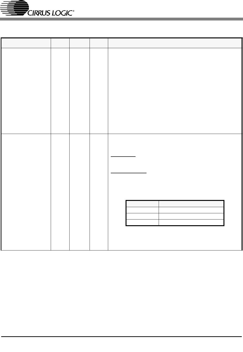
Table 1. Operation Mode Selection
Pin State OPERATING Mode
LOW Hardware Mode
HIGH Parallel Host Mode
VCCIO/2 Serial Host Mode