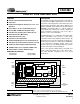
CS61880 Octal E1 Line Interface Unit Features Description Octal E1 Short-haul Line Interface Unit Low Power No External Component Changes for 120 Ω / 75 Ω Operation Pulse Shapes can be customized by the user Internal AMI, or HDB3 Encoding/Decoding LOS Detection per ITU G.775 or ETSI 300- 233 G.772 Non-Intrusive Monitoring G.
CS61880 TABLE OF CONTENTS 1. PIN OUT - 144-PIN LQFP PACKAGE ................................................................................... 7 2. PIN OUT - 160-BALL FBGA PACKAGE .................................................................................. 8 3. PIN DESCRIPTIONS ................................................................................................................ 9 3.1 Power Supplies ............................................................................................
CS61880 10. RECEIVER ............................................................................................................................ 26 10.1 Bipolar Output Mode ...................................................................................................... 26 10.2 Unipolar Output Mode ................................................................................................... 26 10.3 RZ Output Mode ...................................................................................
CS61880 14.33.2 Interrupt Status Registers ............................................................................... 41 15. ARBITRARY WAVEFORM GENERATOR ........................................................................... 42 16. JTAG SUPPORT .................................................................................................................. 43 16.1 TAP Controller ............................................................................................................... 44 16.
CS61880 LIST OF FIGURES Figure 1. CS61880 144-Pin LQFP Package Pin Outs .................................................................... 7 Figure 2. CS61880 160-Ball FBGA Package Pin Outs ................................................................... 8 Figure 3. G.703 BITS Clock Mode in NRZ Mode .......................................................................... 23 Figure 4. G.703 BITS Clock Mode in RZ Mode.............................................................................
CS61880 LIST OF TABLES Table 1. Operation Mode Selection ............................................................................................... 10 Table 2. Mux/Bits Clock Selection ................................................................................................. 11 Table 3. Jitter Attenuation Selection.............................................................................................. 12 Table 4. Cable Impedance Selection ...................................................
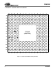
CS61880 144 143 142 141 140 139 138 137 136 135 134 133 132 131 130 129 128 127 126 125 124 123 122 121 120 119 118 117 116 115 114 113 112 111 110 109 TNEG7/UBS7 RCLK7 RPOS7/RDATA7 RNEG7/BPV7 LOS7 RTIP7 RRING7 TV+7 TTIP7 TRING7 TGND7 RRING6 RTIP6 TGND6 TRING6 TTIP6 TV+6 RTIP5 RRING5 TV+5 TTIP5 TRING5 TGND5 RRING4 RTIP4 TGND4 TRING4 TTIP4 TV+4 CLKE TXOE LOS4 RNEG4/BPV4 RPOS4/RDATA4 RCLK4 TNEG4/UBS4 1.
CS61880 2.
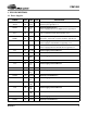
CS61880 3. PIN DESCRIPTIONS 3.1 Power Supplies SYMBOL LQFP FBGA VCCIO 17 92 G1 G14 Power Supply, Digital Interface: Power supply for digital interface pins; typically 3.3 V GNDIO 18 91 G4 G11 Ground, Digital Interface: Power supply ground for the digital interface; typically 0 V RV0+ RV1+ 19 90 H1 H14 Power Supply, Core Circuitry: Power supply for all sub-circuits except the transmit driver; typically +3.
CS61880 3.2 Control SYMBOL MCLK LQFP 10 FBGA E1 TYPE DESCRIPTION I Master Clock Input This pin is a free running reference clock that should be 2.048 MHz. This timing reference is used as follows: - Timing reference for the clock recovery and jitter attenuation circuitry.
CS61880 SYMBOL MUX/BITSEN0 LQFP 43 FBGA K2 TYPE I DESCRIPTION Multiplexed Interface/Bits Clock Select Host Mode -This pin configures the microprocessor interface for multiplexed or non-multiplexed operation. Hardware mode - This pin is used to enable channel 0 as a G.703 BITS Clock recovery channel (Refer to BUILDING INTEGRATED TIMING SYSTEMS (BITS) CLOCK MODE (See Section 8 on page 23). Channel 1 through 7 are not affected by this pin during hardware mode. During host mode the G.
CS61880 SYMBOL WR/DS/SDI RD/RW ALE/AS/SCLK CS/JASEL LQFP 84 85 86 87 FBGA J14 J13 J12 J11 TYPE I I I I DESCRIPTION Write Enable/Data Strobe/Serial Data Intel Parallel Host Mode - This pin, “WR”, functions as a write enable. Motorola Parallel Host Mode - This pin, “DS“, functions as a data strobe input. Serial Host Mode - This pin, “SDI”, functions as the serial data input. Hardware Mode - This pin is not used and should be connected to ground.
CS61880 SYMBOL INTL/MOT/CODEN TXOE CLKE DS450PP3 LQFP 88 114 115 FBGA H12 E14 E13 TYPE DESCRIPTION I Intel/Motorola/Coder Mode Select Input Parallel Host Mode - When this pin is “Low” the microprocessor interface is configured for operation with Motorola processors. When this pin is “High” the microprocessor interface is configured for operation with Intel processors.
CS61880 3.3 Address Inputs/Loopbacks SYMBOL A4 14 LQFP 12 FBGA F4 TYPE DESCRIPTION I Address Selector Input Parallel Host Mode - During non-multiplexed parallel host mode operation, this pin function as the address 4 input for the parallel interface. Hardware Mode - The A4 pin must be tied low at all times.
CS61880 3.4 Cable Select SYMBOL LQFP FBGA TYPE DESCRIPTION Cable Impedance Select Host Mode - The input voltage to this pin does not effect normal operation. Hardware Mode - This pin is used to select the transmitted pulse shape and set the line impedance for all eight receivers and transmitters. This pin also selects whether or not all eight receivers use an internal or external line matching network (Refer to the Table 4 below for proper settings). Table 4.
CS61880 3.6 Digital Rx/Tx Data I/O SYMBOL LQFP FBGA TYPE DESCRIPTION Transmit Clock Input Port 0 - When TCLK is active, the TPOS and TNEG pins function as NRZ inputs that are sampled on the falling edge of TCLK. - If MCLK is active, TAOS will be generated when TCLK is held High for 16 MCLK cycles. TCLK0 36 N1 I NOTE: MCLK is used as the timing reference during TAOS and must have the appropriate stability. - If TCLK is held High in the absence of MCLK, the TPOS and TNEG inputs function as RZ inputs.
CS61880 SYMBOL RCLK0 LQFP 39 FBGA P1 TYPE DESCRIPTION O Receive Clock Output Port 0 - When MCLK is active, this pin outputs the recovered clock from the signal input on RTIP and RRING. In the event of LOS, the RCLK output transitions from the recovered clock to MCLK. - If MCLK is held “High”, the clock recovery circuitry is disabled and the RCLK output is driven by the XOR of RNEG and RPOS. - If MCLK is held “Low”, this output is in a high-impedance state.
CS61880 18 SYMBOL LQFP FBGA TYPE DESCRIPTION RCLK2 78 M14 O Receive Clock Output Port 2 RPOS2/RDATA2 77 M13 O Receive Positive Pulse/ Receive Data Output Port 2 RNEG2/BPV2 76 M12 O Receive Negative Pulse/Bipolar Violation Output Port 2 TCLK3 74 N14 I Transmit Clock Input Port 3 TPOS3/TDATA3 73 N13 I Transmit Positive Pulse/Transmit Data Input Port 3 TNEG3/UBS3 72 N12 I Transmit Negative Pulse/Unipolar-Bipolar Select Port 3 RCLK3 71 P14 O Receive Clock Output Port 3
CS61880 SYMBOL LQFP FBGA TYPE DESCRIPTION RCLK7 143 A1 O Receive Clock Output Port 7 RPOS7/RDATA7 142 A2 O Receive Positive Pulse/ Receive Data Output Port 7 RNEG7/BPV7 141 A3 O Receive Negative Pulse/Bipolar Violation Output Port 7 FBGA TYPE 3.7 Analog RX/TX Data I/O SYMBOL LQFP TTIP0 45 N5 O TRING0 46 P5 O DESCRIPTION Transmit Tip Output Port 0 Transmit Ring Output Port 0 These pins are the differential outputs of the transmit driver.
CS61880 20 SYMBOL LQFP FBGA TYPE DESCRIPTION TRING2 58 M10 O Transmit Ring Output Port 2 RTIP2 60 M8 I Receive Tip Input Port 2 RRING2 61 L8 I Receive Ring Input Port 2 TTIP3 64 N10 O Transmit Tip Output Port 3 TRING3 63 P10 O Transmit Ring Output Port 3 RTIP3 67 P8 I Receive Tip Input Port 3 RRING3 66 N8 I Receive Ring Input Port 3 TTIP4 117 B10 O Transmit Tip Output Port 4 TRING4 118 A10 O Transmit Ring Output Port 4 RTIP4 120 A8 I Receive Tip Input
CS61880 3.8 JTAG Test Interface SYMBOL LQFP FBGA TYPE TRST 95 G12 I TMS 96 F11 I TCK 97 F14 I TDO 98 F13 O TDI 99 F12 I SYMBOL LQFP FBGA TYPE REF 94 H13 I DESCRIPTION JTAG Reset This active Low input resets the JTAG controller. This input is pulled up internally and may be left as a NC when not used. JTAG Test Mode Select Input This input enables the JTAG serial port when active High. This input is sampled on the rising edge of TCK.
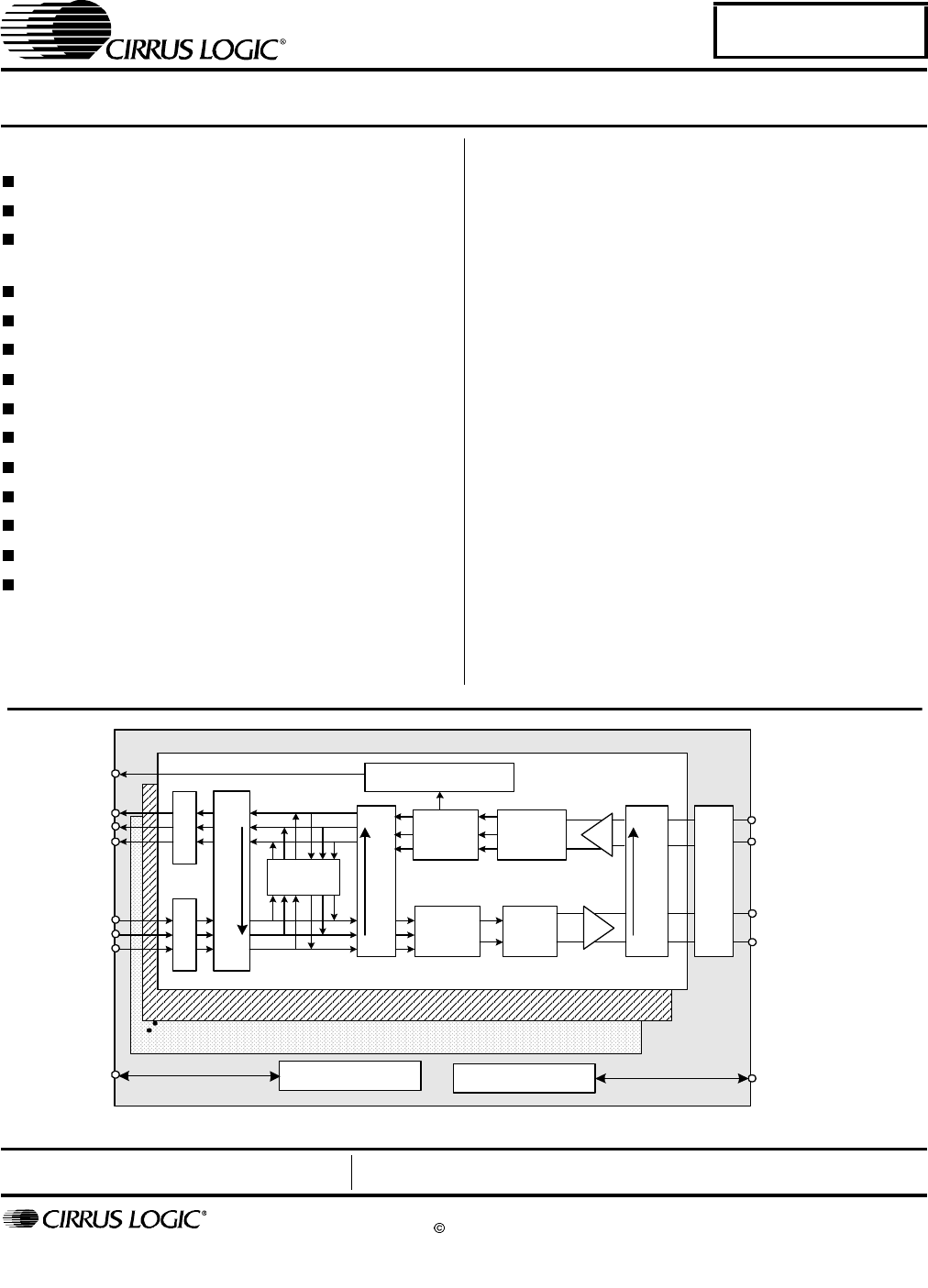
CS61880 4. OPERATION 7. G.772 MONITORING The CS61880 is a full featured line interface unit for up to eight E1 75 Ω or E1 120 Ω lines. The device provides an interface to twisted pair or co-axial media. A matched impedance technique is employed that reduces power and eliminates the need for matching resistors. As a result, the device can interface directly to the line through a transformer without the need for matching resistors on the transmit side.
CS61880 8. BUILDING INTEGRATED TIMING SYSTEMS (BITS) CLOCK MODE This mode is used to enable one or more channels as a stand-alone timing recovery unit used for G.703 Clock Recovery. In host mode, each channel can be setup as an independent G.703 timing recovery unit, through the Bits Clock Enable Register (1Eh) (See Section 14.31 on page 40), setting the desired bit to “1” enables BITS Clock mode for that channel. The following diagrams show how the BITS clock function operates.
CS61880 9. TRANSMITTER The CS61880 contains eight identical transmitters that each use a low power matched impedance driver to eliminate the need for external load matching resistors, while providing superior return loss. As a result, the TTIP/TRING outputs can be connected directly to the transformer allowing one hardware circuit for E1 120 Ω, and E1 75 Ω applications.
CS61880 TNEG/UBS “High” for more than 16 TCLK cycles. Transmit data is input to the part via the TPOS/TDATA pin on the falling edge of TCLK. When operating the part in hardware mode, the CODEN pin is used to select between HDB3 or AMI encoding. During host mode operation, the line coding is selected via the Line Length Channel ID Register (10h) (See Section 14.17 on page 38). NOTE: The encoders/decoders are selected for all eight channels in both hardware and host mode. 9.
CS61880 10. RECEIVER The CS61880 contains eight identical receivers that utilize an internal matched impedance technique that provides for the use of a common set of external components for 120 Ω (E1), and 75 Ω (Ε1) operation (Refer to Figure 16 on page 50). This feature enables the use of a one stuffing option for all E1 line impedances. The receivers can also be configured to use different external resistors to match the line impedance for E1 75 Ω or E1 120 Ω modes (Refer to Figure 17 on page 51).
CS61880 10.4 Receiver Powerdown/High-Z All eight receivers are powered down when MCLK is held low. In addition, this will force the RCLK, RPOS/RDATA and RNEG outputs into a high impedance state. 10.5 Loss-of-Signal (LOS) The CS61880 makes use of both analog and digital LOS detection circuitry that is compliant to the latest specifications. The LOS condition can be set to either ITU G.775 or ETSI 300 233. This change is done through the LOS/AIS Mode Enable Register (0Dh) (See Section 14.14 on page 37).
CS61880 11. JITTER ATTENUATOR The CS61880 internal jitter attenuators can be switched into either the receive or transmit paths. Alternatively, it can be removed from both paths to reduce the propagation delay. During Hardware mode operation, the location of the jitter attenuator for all eight channels are controlled by the JASEL pin (Refer to Table 7 for pin configurations). The jitter attenuator’s FIFO length and corner frequency, can not be changed in hardware mode.
CS61880 12. OPERATIONAL SUMMARY A brief summary of the CS61880 operations in hardware and host mode is provided in Table 8. Table 8.
RCLK Jitter RNEG Attenuator RPOS Jitter TCLK Transmit Control & Pulse Shaper Attenuator TNEG Decoder TPOS Encoder CS61880 Clock Recovery & Data Recovery TTIP TRING RTIP RRING Figure 7. Analog Loopback Block Diagram MCLK TCLK Jitter TNEG Attenuator TPOS Encoder TAOS Transmit Control & Pulse Shaper TTIP TRING RCLK Jitter Attenuator RPOS RNEG Decoder (All One's) Clock Recovery & Data Recovery RTIP RRING Figure 8. Analog Loopback with TAOS Block Diagram 12.
RPOS RNEG RCLK Jitter Attenuator TCLK Transmit Control & Pulse Shaper Jitter Attenuator TNEG Encoder TPOS Decoder CS61880 Clock Recovery & Data Recovery TTIP TRING RTIP RRING Figure 9.
CS61880 13. HOST MODE 13.2 Serial Port Operation Host mode allows the CS61880 to be configured and monitored using an internal register set. (Refer to Table 1, “Operation Mode Selection,” on page 10). The term, “Host mode” applies to both Parallel Host and Serial Host modes. Serial port host mode operation is selected when the MODE pin is left open or set to VCC/2.
CS61880 bidirectional I/O port, SDI and SDO may be tied together. in Figure 28, Figure 26, Figure 25, Figure 27, Figure 29, Figure 30, Figure 31 and Figure 32. As illustrated in Figure 12, the ACB consists of a R/W bit, address field, and two reserved bits. The R/W bit specifies if the current register access is a read (R/W = 1) or a write (R/W = 0) operation. The address field specifies the register address from 0x00 to 0x1f.
CS61880 three bits of the parallel address are don’t cares on the CS61880, they should be set to zero for proper operation. 13.4 Register Set The register set available during host mode operations are presented in Table 10. While the upper Table 10.
CS61880 14. REGISTER DESCRIPTIONS 14.1 Revision/IDcode Register (00h) BIT [7:4] NAME REVI 7-4 [3:0] REVI 3-0 Description Bits [7:4] are taken from the least-significant nibble of the Device IDCode, which are 0000. (Refer to Device ID Register (IDR) (See Section 16.3 on page 47). Bits [3:0] are the revision bits from the JTAG IDCODE register, CS61880 Revision A = 0000. These bits are subject to change with the revision of the device (Refer to Device ID Register (IDR) (See Section 16.3 on page 47). 14.
CS61880 14.7 LOS Interrupt Enable Register (06h) BIT [7:0] NAME Description LOSE 7-0 Any change in a LOS Status Register will cause the INT pin to go low if corresponding bit in this register is set to “1”. Register bits default to 00h after power-up or reset. 14.8 DFM Interrupt Enable Register (07h) BIT [7:0] NAME Description Enables interrupts for failures detected by the DFM.
CS61880 14.14 LOS/AIS Mode Enable Register (0Dh) BIT [7:0] NAME Description LAME 7-0 Setting bit n to “1” enables ETSI 300 233 compliant LOS/AIS for channel n; setting bit n to “0” enables ITU G.775 compliant LOS/AIS for channel n. Register bits default to 00h after power-up or reset. 14.15 Automatic TAOS Register (0Eh) BIT [7:0] NAME Description ATAO 7-0 Setting bit n to “1” enables automatic TAOS generation on channel n when LOS is detected. Register bits default to 00h after power-up or reset. 14.
CS61880 14.17 Line Length Channel ID Register (10h) BIT [7:3] NAME RSVD 7-3 [2:0] LLID 2-0 Description RESERVED (These bits must be set to 0.) The value written to these bits specify the LIU channel for which the Pulse Shape Configuration Data (register 11h) applies. For example, writing a value of a binary 000 to the 3-LSBs will select channel 0. The pulse shape configuration data for the channel specified in this register are written or read through the Line Length Data Register (11h).
CS61880 14.21 AIS Interrupt Enable Register (14h) BIT [7:0] NAME AISE 7-0 Description This register enables changes in the AIS Status register to be reflected in the AIS Interrupt Status register, thus causing an interrupt on the INT pin. Register bits default to 00h after power-up or reset. 14.22 AIS Interrupt Status Register (15h) BIT NAME [7:0] AISI 7-0 Description Bit n is set to “1” to indicate a change of status of bit n in the AIS Status Register.
CS61880 14.26 AWG Enable Register (19h) BIT [7:0] NAME Description The AWG enable register is used for selecting the source of the customized transmission pulse-shape. Setting bit n to “1” in this register selects the AWG as the source of the output AWGN 7-0 pulse shape for channel n. When bit n is set to “0” the pre-programmed pulse shape in the ROM is selected for transmission on channel n. (Refer to Arbitrary Waveform Generator (See Section 15 on page 42).
CS61880 14.33.1 Interrupt Enable Registers The Interrupt Enable registers: LOS Interrupt Enable Register (06h) (See Section 14.7 on page 36), DFM Interrupt Enable Register (07h) (See Section 14.8 on page 36), AIS Interrupt Enable Register (14h) (See Section 14.21 on page 39), enable changes in status register state to cause an interrupt on the INT pin. Interrupts are maskable on a per channel basis.
CS61880 15. ARBITRARY WAVEFORM GENERATOR Using the Arbitrary Waveform Generator (AWG) allows the user to customize the transmit pulse shapes to compensate for nonstandard cables, transformers, protection circuitry, or to reduce power consumption by reducing the output pulse amplitude. A channel is configured for a custom pulse shape by enabling the AWG for that channel and then storing data representing the pulse shape into the 24 phase sample locations.
CS61880 sample address (00000 binary) needs to be written to the AWG Phase Address Register (17h) (See Section 14.24 on page 39), and each subsequent access (read or write) to the AWG Phase Data Register (18h) (See Section 14.25 on page 39) will automatically increment the phase sample address. The channel address, however, remains unaffected by the Auto-Increment mode. The AWG Phase Address Register (17h) (See Section 14.
CS61880 Digital output pins Digital input pins JTAG BLOCK parallel latched output Boundary Scan Data Register TDI Device ID Data Register MUX TDO Bypass Data Register Instruction (shift) Register TCK parallel latched output TMS TAP Controller Figure 14. Test Access Port Architecture 16.1 TAP Controller 16.1.4 Select-DR-Scan The TAP Controller is a 16 state synchronous state machine clocked by the rising edge of TCK. The TMS input governs state transitions as shown in Figure 15.
CS61880 1 Test-Logic-Reset 0 0 Run-Test/Idle 1 Select-DR-Scan 1 Select- I R-Scan 0 0 1 1 Capture-DR Capture- IR 0 0 0 Shift-DR 1 1 Exit1-DR Exit1- IR 1 0 0 0 Pause-DR Pause- IR 1 0 1 0 Exit2-DR Exit2- IR 1 1 Update-DR 1 0 Shift- IR 1 0 1 Update- IR 0 1 0 Figure 15. TAP Controller State Diagram 16.1.8 Pause-DR The pause state allows the test controller to temporarily halt the shifting of data through the current test data register. 16.1.
CS61880 16.1.14 Exit1-IR This is a temporary state. The test data register selected by the current instruction retains its previous value. 16.1.15 Pause-IR The pause state allows the test controller to temporarily halt the shifting of data through the instruction register. 16.1.16 Exit2-IR This is a temporary state. The test data register selected by the current instruction retains its previous value. 16.1.
CS61880 16.3 Device ID Register (IDR) Revision section: 0h = Rev A, 1h = Rev B and so on. The device Identification Code [27 - 12] is derived from the last three digits of the part number (880). The LSB is a constant 1, as defined by IEEE 1149.1.
CS61880 Table 14.
CS61880 Table 14.
CS61880 18. APPLICATIONS +3.3V 0.1 µ F 0.1 µ F Note 1 Note 1 + + 68 µ F Note 2 TGND RGND RV+ TV+ R TIP 0.1 µ F +3.3V R1 RECEIVE LINE VCCIO 0.1 µ F R2 + R RIN G T1 1:2 GNDIO 75 Ω Cable CS61880 One Channel T RIN G TRANSMIT LINE T TIP +3.3V T2 1:1.15 13.3k Ω NC 120 Ω Cable CBLSEL REF GND Component R1 (Ω) R2 (Ω) E1 75Ω Coaxial Cable 15 15 E1 120Ω Twisted Pair Cable 15 15 Notes:1) Required Capacitor between each TV+, RV+, VCCIO and TGND, RGND, GNDIO respectively.
CS61880 +3.3V 0.1 µ F 0.1 µ F Note 1 Note 1 + + 68 µ F Note 2 TGND RGND RV+ 1kΩ TV+ R TIP +3.3V R1 0.1 µ F RECEIVE LINE VCCIO 0.1µ F R2 + R RIN G T1 1:2 1kΩ GNDIO CS61880 One Channel T RIN G TRANSMIT LINE T TIP T2 1:1.15 120 Ω Cable CBLSEL NC REF 75 Ω Cable GND GND Component R1 (Ω) R2 (Ω) Notes: 13.3k Ω E1 75 Ω Coaxial Cable 9.31 9.31 E1 120 Ω Twisted Pair Cable 15 15 1)Required Capacitor between each TV+, RV+, VCCIO and TGND, RGND, GNDIO respectively.
CS61880 18.1 Transformer Specifications 18.2 Crystal Oscillator Specifications Recommended transformer specifications are shown in Table 15. Any transformer used with the CS61880 should meet or exceed these specifications. When a reference clock signal is not available, a CMOS crystal oscillator may be used as the reference clock signal. The oscillator must have a minimum symmetry of 40-60% and minimum stability of + 100 ppm. Table 15.
CS61880 19. CHARACTERISTICS AND SPECIFICATIONS 19.1 Absolute Maximum Ratings CAUTION: Operations at or beyond these limits may result in permanent damage to the device. Normal operation is not guaranteed at these extremes. Parameter DC Supply (referenced to RGND = TGND = 0V) DC Supply Symbol Min. Max Units RV+ TV+ - 4.0 4.0 V V VCCIO -0.5 4.6 V Input Voltage, Any Digital Pin except CBLSEL, MODE and LOOP(n) pins (referenced to GNDIO = 0V) VIH GNDIO -0.5 5.
CS61880 19.3 Digital Characteristics (TA = -40° C to 85° C; TV+, RV+ = 3.3 V ±5%; GND = 0 V) Parameter Symbol Min. Typ Max Units High-Level Input Voltage Note 6 VIH 2.0 - - V Low-Level Input Voltage Note 6 VIL - - 0.8 V LOOP[7:0] Low-Level Input Voltage VIHL - - 1/3 VCCIO-0.2 V LOOP[7:0] Mid-Level Input Voltage VIHM 1/3 VCCIO +0.2 1/2 VCCIO 2/3 VCCIO-0.2 V LOOP[7:0] High-Level Input Voltage VIHH 2/3 VCCIO +0.
CS61880 19.5 Receiver Analog Characteristics (TA = -40° C to 85° C; TV+, RV+ = 3.3 V ±5%; GND = 0 V)) Parameter Min. Allowable Cable Attenuation @ 1024 kHz Typ Max Units - - - 12 dB RTIP/RRING Input Impedance (Internal Line matching mode) Note 10 E1 120 Ω Load E1 75 Ω Load - 13k 50 - Ω RTIP/RRING Input Impedance (External Line matching mode) Note 10 E1 120 Ω Load E1 75 Ω Load - 13k 13k - Ω 0.5 - - Vp -18 - Receiver Dynamic Range Signal to Noise margin (Per G.
CS61880 19.6 Jitter Attenuator Characteristics (TA = -40° C to 85° C; TV+, RV+ = 3.3 V ±5%; GND = 0 V) Parameter Min. Typ Max Units - 1.25 2.50 - Hz + 0.5 -19.
CS61880 1000 300 TYP. E1 Performance PEAK TO PEAK JITTER (UI) 138 100 28 18 10 ITU G.823 1.5 1 .4 .2 .1 1 1.8 4.9 10 20 100 300 1k 2.4k 10k 18k 100k FREQUENCY IN Hz Figure 19. Jitter Tolerance Characteristic vs. G.
CS61880 19.7 Master Clock Switching Characteristics Parameter Symbol Min. Typ Max Units MASTER CLOCK (MCLK) Master Clock Frequency MCLK 2.048 MHz Master Clock Tolerance - -100 +100 ppm Master Clock Duty Cycle - 40 50 60 % Symbol Min. Typ Max Units 19.8 Transmit Switching Characteristics Parameter - 2.
CS61880 RCLK th tsu RPOS/RNEG CLKE = 1 th tsu RPOS/RNEG CLKE = 0 Figure 20. Recovered Clock and Data Switching Characteristics tpw2 tpwh2 TCLK tsu2 th2 TPOS/TNEG Figure 21. Transmit Clock and Data Switching Characteristics tr tf 90% 90% Any Digital Output 10% 10% Figure 22.
CS61880 19.10 Switching Characteristics - Serial Port Parameter Symbol Min. Typ.
CS61880 19.11 Switching Characteristics - Parallel Port (Multiplexed Mode) Parameter Ref. # Min. Typ.
CS61880 1 ALE 12 4 7 WR 6 5 CS 3 2 D[7:0] 8 ADDRESS 9 Write Data 15 14 HIGH-Z HIGH-Z RDY 13 Figure 25. Parallel Port Timing - Write; Intel® Multiplexed Address / Data Bus Mode 1 ALE 12 4 7 RD 6 5 CS 2 D[7:0] 3 11 10 ADDRESS Read Data 15 14 HIGH-Z HIGH-Z RDY 13 Figure 26.
CS61880 1 AS 4 12 7 DS R/W 5 6 CS 8 3 2 ADDRESS D[7:0] 9 Write Data 17 18 HIGH-Z HIGH-Z ACK 16 Figure 27. Parallel Port Timing - Write; Motorola® Multiplexed Address / Data Bus Mode 1 AS 4 12 7 DS R/W 6 5 CS 3 2 10 11 ADDRESS D[7:0] Read Data 17 18 HIGH-Z HIGH-Z ACK 16 Figure 28.
CS61880 19.12 Switching Characteristics- Parallel Port (Non-Multiplexed Mode) Parameter Ref. # Min. Typ.
CS61880 2 1 ADDRESS A[4:0] ALE (pulled high) 5 WR 3 4 CS 6 7 Write Data D[7:0] 11 12 HIGH-Z HIGH-Z RDY 10 Figure 29. Parallel Port Timing - Write; Intel Non-Multiplexed Address / Data Bus Mode 2 1 A[4:0] ALE ADDRESS (pulled high) 5 RD 3 4 CS 8 9 D[7:0] Read Data 11 HIGH-Z 12 HIGH-Z RDY 10 Figure 30.
CS61880 1 2 A[4:0] ADDRESS AS (pulled high) 5 DS R/W 3 4 CS 6 7 Write Data D[7:0] 14 15 HIGH-Z HIGH-Z ACK 13 Figure 31. Parallel Port Timing - Write; Motorola Non-Multiplexed Address / Data Bus Mode 1 2 A[4:0] AS ADDRESS (pulled high) 5 DS R/W 3 4 CS 8 9 Read Data D[7:0] 14 15 HIGH-Z HIGH-Z ACK 13 Figure 32.
CS61880 19.13 Switching Characteristics - JTAG Parameter Symbol Min. Max Units Cycle Time tcyc 200 - ns TMS/TDI to TCK Rising Setup Time tsu 50 - ns TCK Rising to TMS/TDI Hold Time th 50 - ns TCK Falling to TDO Valid tdv - 70 ns tcyc TCK tsu th TMS TDI tdv TDO Figure 33.
CS61880 20. COMPLIANT RECOMMENDATIONS AND SPECIFICATIONS ETSI ETS 300-011 ITU-T G.732 ETSI ETS 300-166 ITU-T G.735 ETSI ETS 300-233 ITU-T G.736 ETSI TBR 12/13 ITU-T G.742 IEEE 1149.1 ITU-T G.772 ITU-T I.431 ITU-T G.775 ITU-T G.703 ITU-T G.783 ITU-T G.704 ITU-T G.823 ITU-T G.706 ITU-T O.
CS61880 21. 160-BALL FBGA PACKAGE DIMENSIONS Figure 34.
CS61880 22. 144-PIN LQFP PACKAGE DIMENSIONS E E1 D D1 1 e B ∝ A A1 L Figure 35. 144-Pin LQFP Package Drawing Table 16. 144-Pin Package Dimensions INCHES MILLIMETERS MIN NOM MAX MIN NOM --0.55 0.063 --1.40 0.002 0.004 0.006 0.05 0.10 0.007 0.008 0.011 0.17 0.20 0.854 0.866 BSC 0.878 21.70 22.0 BSC 0.783 0.787 BSC 0.791 19.90 20.0 BSC 0.854 0.866 BSC 0.878 21.70 22.0 BSC 0.783 0.787 BSC 0.791 19.90 20.0 BSC 0.016 0.020 0.024 0.40 0.50 BSC 0.000° 4° 7.000° 0.00° 4° ∝ L 0.018 0.024 0.030 0.45 0.