
Instruction Manual
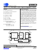
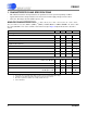
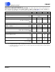
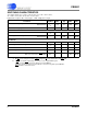
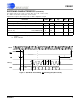
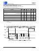
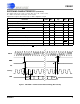
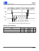
Table Of Contents
- Features & Description
- General Description
- Table of Contents
- List of Figures
- List of Tables
- 1. Characteristics and Specifications
- 2. Overview
- 3. Theory of Operation
- 3.1 Converter Operation
- 3.2 Clock
- 3.3 Voltage Reference
- 3.4 Analog Input
- 3.5 Output Coding Format
- 3.6 Typical Connection Diagrams
- 3.7 AIN & VREF Sampling Structures
- 3.8 Converter Performance
- 3.9 Digital Filter Characteristics
- 3.10 Serial Port
- 3.11 Power Supplies & Grounding
- 3.12 Using the CS5581 in Multiplexing Applications
- 3.13 Synchronizing Multiple Converters
- 4. Pin Descriptions
- 5. Package Dimensions
- 6. Ordering Information
- 7. Environmental, Manufacturing, & Handling Information
- 8. Revision History
CS5581
DS796PP1 7
3/25/08
14:34
SWITCHING CHARACTERISTICS (CONTINUED)
T
A
= -40 to +85 °C; V1+ = V2+ = +2.5 V, ±5%; V1- = V2- = -2.5 V, ±5%;
VL - VLR = 3.3 V, ±5%, 2.5 V, ±5%, or 1.8 V, ±5%
Input levels: Logic 0 = 0V = Low; Logic 1 = VD+ = High; CL = 15 pF.
11. SDO and SCLK will be high impedance when CS is high. In some systems SCLK and SDO may require pull-down
resistors.
12. SCLK = MCLK/2.
Parameter Symbol Min Typ Max Unit
Serial Port Timing in SSC Mode (SMODE = VL)
RDY
falling to MSB stable t
1
--2-MCLKs
Data hold time after SCLK rising t
2
-10-ns
Serial Clock (Out) Pulse Width (low)
(Note 11, 12) Pulse Width (high)
t
3
t
4
50
50
-
-
-
-
ns
ns
RDY
rising after last SCLK rising t
5
-8-MCLKs
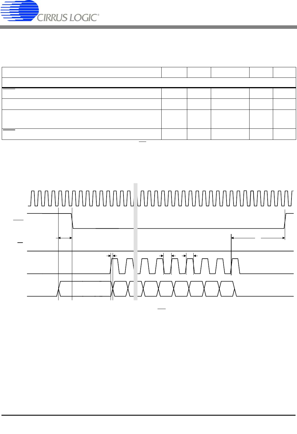
MCLK
RDY
SCLK(o)
SDO
MSB MSB–1
LSB
LSB+1
CS
t
1
t
2
t
3
t
4
t
5
Figure 1. SSC Mode - Read Timing, CS remaining low (Not to Scale)