
Instruction Manual
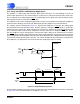
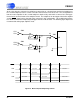
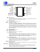
Table Of Contents
- Features & Description
- General Description
- Table of Contents
- List of Figures
- List of Tables
- 1. Characteristics and Specifications
- 2. Overview
- 3. Theory of Operation
- 3.1 Converter Operation
- 3.2 Clock
- 3.3 Voltage Reference
- 3.4 Analog Input
- 3.5 Output Coding Format
- 3.6 Typical Connection Diagrams
- 3.7 AIN & VREF Sampling Structures
- 3.8 Converter Performance
- 3.9 Digital Filter Characteristics
- 3.10 Serial Port
- 3.11 Power Supplies & Grounding
- 3.12 Using the CS5581 in Multiplexing Applications
- 3.13 Synchronizing Multiple Converters
- 4. Pin Descriptions
- 5. Package Dimensions
- 6. Ordering Information
- 7. Environmental, Manufacturing, & Handling Information
- 8. Revision History
CS5581
30 DS796PP1
3/25/08
14:34
SCLK – Serial Clock Input/Output, Pin 23
The SMODE pin determines whether the SCLK signal is an input or an output signal. SCLK
determines the rate at which data is clocked out of the SDO pin. If the converter is in SSC
mode, the SCLK frequency will be determined by the master clock frequency of the converter
(either MCLK or the internal oscillator). In SEC mode, the user determines the SCLK frequency.
If SCLK is an output (SMODE = VL), it will be in a high-impedance state when CS
is high.
RDY
– Ready, Pin 24
At the end of any conversion RDY
falls to indicate that a conversion word has been placed into
the serial port. RDY
will return high after all data bits are shifted out of the serial port or two mas-
ter clock cycles before new data becomes available if the CS
pin is inactive (high); or two mas-
ter clock cycles before new data becomes available if the user holds CS
low but has not started
reading the data from the converter when in SEC mode.