
Instruction Manual
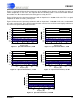
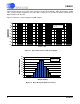
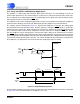
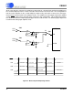
Table Of Contents
- Features & Description
- General Description
- Table of Contents
- List of Figures
- List of Tables
- 1. Characteristics and Specifications
- 2. Overview
- 3. Theory of Operation
- 3.1 Converter Operation
- 3.2 Clock
- 3.3 Voltage Reference
- 3.4 Analog Input
- 3.5 Output Coding Format
- 3.6 Typical Connection Diagrams
- 3.7 AIN & VREF Sampling Structures
- 3.8 Converter Performance
- 3.9 Digital Filter Characteristics
- 3.10 Serial Port
- 3.11 Power Supplies & Grounding
- 3.12 Using the CS5581 in Multiplexing Applications
- 3.13 Synchronizing Multiple Converters
- 4. Pin Descriptions
- 5. Package Dimensions
- 6. Ordering Information
- 7. Environmental, Manufacturing, & Handling Information
- 8. Revision History
CS5581
22 DS796PP1
3/25/08
14:34
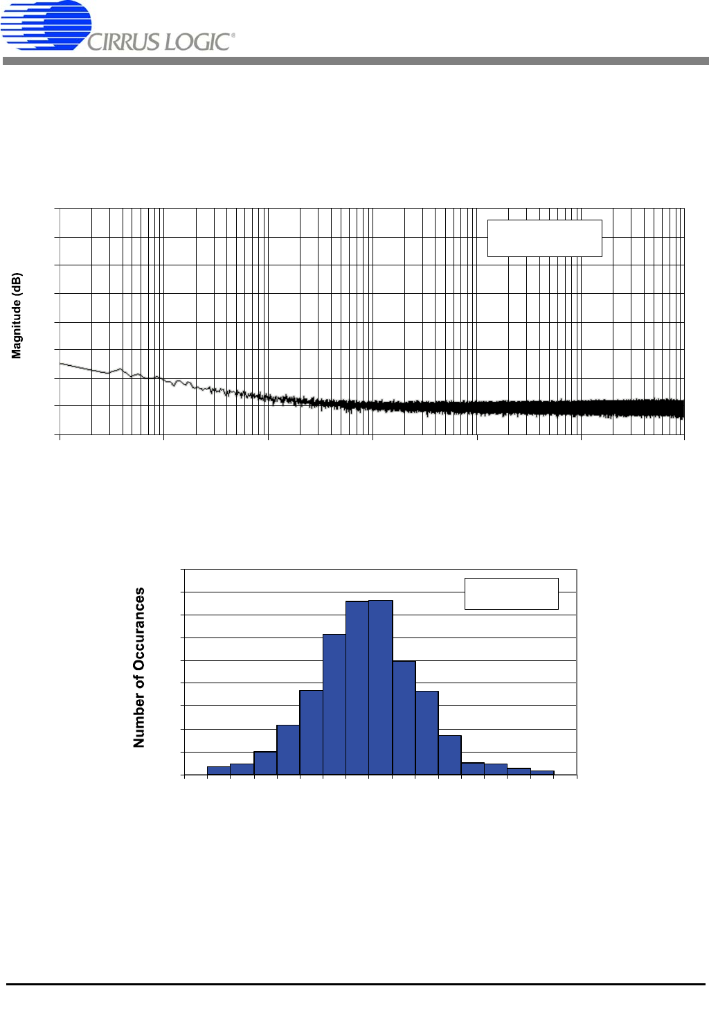
Figure 16 illustrates the noise floor of the converter from 0.1 Hz to 100 kHz. While the plot does exhibit
some 1/f noise at lower frequencies, the noise floor is entirely free of spurious frequency content due to
digital activity inside the chip.
Figure 17 illustrates a noise histogram of 4096 samples.
-160
-140
-120
-100
-80
-60
-40
-20
0
0.1 1 10 100 1k 10k
100k
Frequency (Hz)
Shorted Input
2M Samples @ 200 kSps
16 Averages
Figure 16. Spectral Plot of Noise with Shorted Input
0
100
200
300
400
500
600
700
800
900
-8-7-6-5-4-3-2-1012345678
Mean = -0.61
Std. Dev = 2.33
Output (Codes)
Figure 17. Noise Histogram (4096 Conversions)