
Instruction Manual
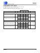
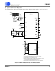
Table Of Contents
- Features & Description
- General Description
- Table of Contents
- List of Figures
- List of Tables
- 1. Characteristics and Specifications
- 2. Overview
- 3. Theory of Operation
- 3.1 Converter Operation
- 3.2 Clock
- 3.3 Voltage Reference
- 3.4 Analog Input
- 3.5 Output Coding Format
- 3.6 Typical Connection Diagrams
- 3.7 AIN & VREF Sampling Structures
- 3.8 Converter Performance
- 3.9 Digital Filter Characteristics
- 3.10 Serial Port
- 3.11 Power Supplies & Grounding
- 3.12 Using the CS5581 in Multiplexing Applications
- 3.13 Synchronizing Multiple Converters
- 4. Pin Descriptions
- 5. Package Dimensions
- 6. Ordering Information
- 7. Environmental, Manufacturing, & Handling Information
- 8. Revision History
CS5581
DS796PP1 17
3/25/08
14:34
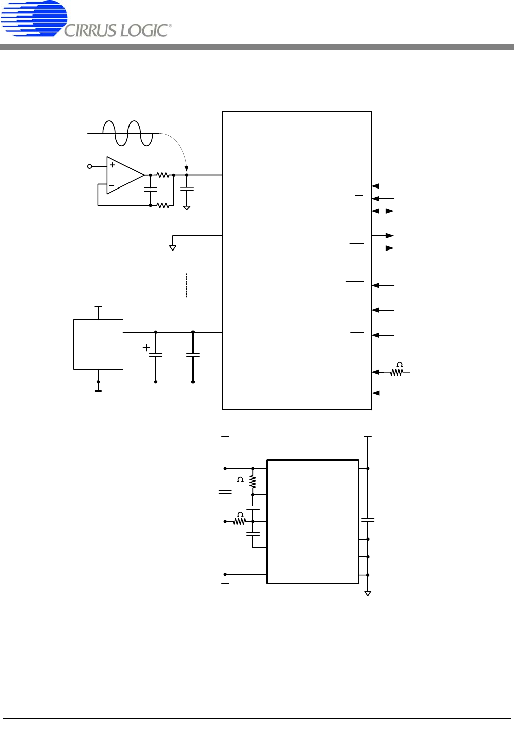
3.6 Typical Connection Diagrams
The following figure depicts the CS5581 powered from bipolar analog supplies, +2.5 V and - 2.5 V.
Figure 6. CS5581 Configured Using ±2.5V Analog Supplies
VREF-
VREF+
+4.096
Voltage
Reference
(NOTE 1)
ACOM
AIN
+2.5 V
SMODE
CS
5
SCLK
5
SDO
RDY
CONV
MCLK
RST
BP/UP
1. See Section 3.3 Voltage Reference for information on required
voltage reference performance criteria.
2.Locate capacitors so as to minimize loop length.
3. The ±2.5 V supplies should also be bypassed to ground at the converter.
4. VLR and the power supply ground for the ±2.5 V should be
connected to the same ground plane under the chip.
5. SCLK and SDO may require pull-down resistors in some applications.
NOTES
-2.5 V
BUFEN
(V-) Buffers Off
(V+) Buffers On
10 µF0.1 µF
V1+
V2+
V1-
V2-
VL
VLR
DCR
+2.5 V
+3.3 V to +1.8 V
0.1 µF
0.1 µF
X7R
0.1 µF
10
49.9
150pF
2k
4700pF
C0G
-2.048 V
+2.048 V
0 V
-2.5 V
CS5571
TST
10
0.1 µF
VLR2
50
VLR3
CS3003
CS5581