
Instruction Manual
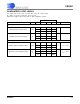
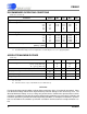
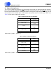
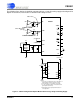
Table Of Contents
- Features & Description
- General Description
- Table of Contents
- List of Figures
- List of Tables
- 1. Characteristics and Specifications
- 2. Overview
- 3. Theory of Operation
- 3.1 Converter Operation
- 3.2 Clock
- 3.3 Voltage Reference
- 3.4 Analog Input
- 3.5 Output Coding Format
- 3.6 Typical Connection Diagrams
- 3.7 AIN & VREF Sampling Structures
- 3.8 Converter Performance
- 3.9 Digital Filter Characteristics
- 3.10 Serial Port
- 3.11 Power Supplies & Grounding
- 3.12 Using the CS5581 in Multiplexing Applications
- 3.13 Synchronizing Multiple Converters
- 4. Pin Descriptions
- 5. Package Dimensions
- 6. Ordering Information
- 7. Environmental, Manufacturing, & Handling Information
- 8. Revision History
CS5581
12 DS796PP1
3/25/08
14:34
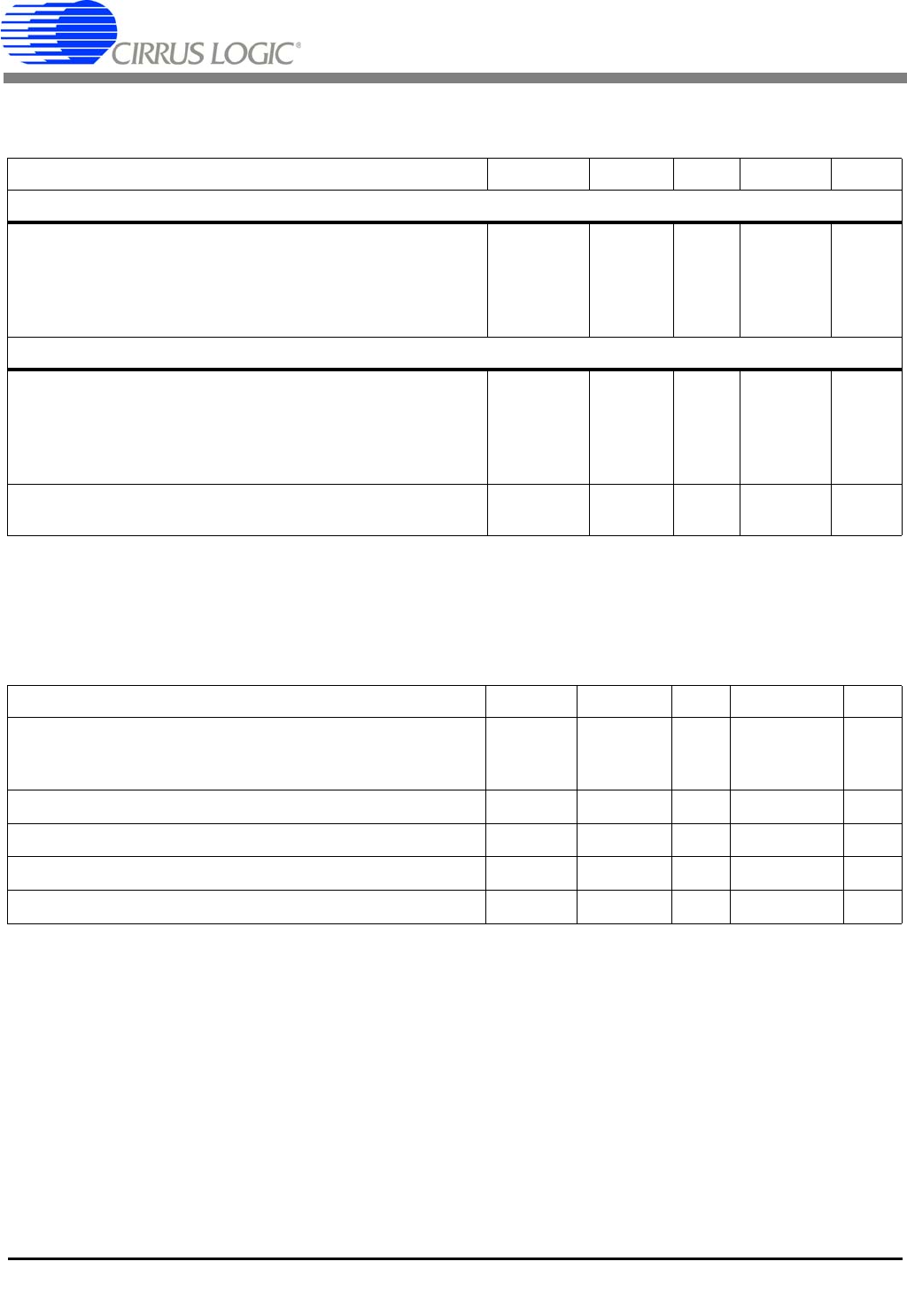
RECOMMENDED OPERATING CONDITIONS
(VLR = 0V, see Note 16)
16. The logic supply can be any value VL – VLR = +1.71 to +3.465 volts as long as VLR ≥ V2- and VL ≤ 3.465 V.
17. The differential voltage reference magnitude is constrained by the V1+ or V1- supply magnitude.
ABSOLUTE MAXIMUM RATINGS
(VLR = 0V)
Notes:
18. V1+ = V2+; V1- = V2-
19. V1- = V2-
20. Transient currents of up to 100 mA will not cause SCR latch-up.
WARNING:
Recommended Operating Conditions indicate limits to which the device is functionally operational. Abso-
lute Maximum Ratings indicate limits beyond which permanent damage to the device may occur. The
Absolute Maximum Ratings are stress ratings only and the device should not be operated at these limits.
Operation at conditions beyond the Recommended Operating Conditions may affect device reliability, and
functional operation beyond Recommended Operating Conditions is not implied. Performance specifica-
tions are intended for the conditions specified for each table in the Characteristics and Specifications sec-
tion.
Parameter Symbol Min Typ Max Unit
Single Analog Supply
DC Power Supplies: (Note 16)
V1+
V2+
V1-
V2-
V1+
V2-
V1+
V2-
4.75
4.75
-
-
5.0
5.0
0
0
5.25
5.25
-
-
V
V
V
V
Dual Analog Supplies
DC Power Supplies: (Note 16)
V1+
V2+
V1-
V2-
V1+
V2-
V1+
V2-
+2.375
+2.375
-2.375
-2.375
+2.5
+2.5
-2.5
-2.5
+2.625
+2.625
-2.625
-2.625
V
V
V
V
Analog Reference Voltage (Note 17)
[VREF+] – [VREF-]
VREF 2.4 4.096 4.2 V
Parameter Symbol Min Typ Max Unit
DC Power Supplies:
[V1+] – [V1-] (Note 18)
VL + [ |V1-| ] (Note 19)
-
-
0
0
-
-
5.5
6.1
V
V
Input Current, Any Pin Except Supplies (Note 20) I
IN
--±10mA
Analog Input Voltage (AIN and VREF pins) V
INA
(V1-) – 0.3 - (V1+) + 0.3 V
Digital Input Voltage V
IND
VLR – 0.3 - VL + 0.3 V
Storage Temperature T
stg
-65 - 150 °C