
Instruction Manual
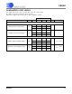
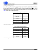
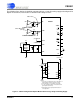
Table Of Contents
- Features & Description
- General Description
- Table of Contents
- List of Figures
- List of Tables
- 1. Characteristics and Specifications
- 2. Overview
- 3. Theory of Operation
- 3.1 Converter Operation
- 3.2 Clock
- 3.3 Voltage Reference
- 3.4 Analog Input
- 3.5 Output Coding Format
- 3.6 Typical Connection Diagrams
- 3.7 AIN & VREF Sampling Structures
- 3.8 Converter Performance
- 3.9 Digital Filter Characteristics
- 3.10 Serial Port
- 3.11 Power Supplies & Grounding
- 3.12 Using the CS5581 in Multiplexing Applications
- 3.13 Synchronizing Multiple Converters
- 4. Pin Descriptions
- 5. Package Dimensions
- 6. Ordering Information
- 7. Environmental, Manufacturing, & Handling Information
- 8. Revision History
CS5581
DS796PP1 11
3/25/08
14:34
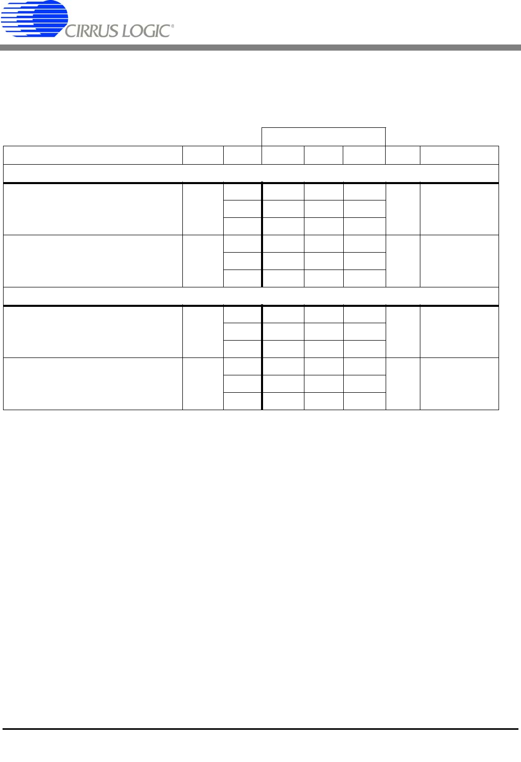
GUARANTEED LOGIC LEVELS
T
A
=-40to+85°C;V1+=V2+=+2.5V, ±5%; V1- = V2- = -2.5 V, ±5%;
VL - VLR = 3.3 V, ±5%, 2.5 V, ±5%, or 1.8 V, ±5%
Input levels: Logic 0 = 0V = Low; Logic 1 = VD+ = High; CL = 15 pF.
Guaranteed Limits
Parameter Sym VL Min Typ Max Unit Conditions
Logic Inputs
Minimum High-level Input Voltage:
V
IH
3.3 1.9
V2.5 1.6
1.8 1.2
Maximum Low-level Input Voltage:
V
IL
3.3 1.1
V2.5 0.95
1.8 0.6
Logic Outputs
Minimum High-level Output Voltage:
V
OH
3.3 2.9
V
I
OH
=-2mA
2.5 2.1
1.8 1.65
Maximum Low-level Output Voltage:
V
OL
3.3 0.36
V
I
OH
=-2mA
2.5 0.36
1.8 0.44