
Instruction Manual
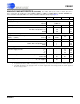
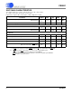
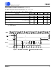
Table Of Contents
- Features & Description
- General Description
- Table of Contents
- List of Figures
- List of Tables
- 1. Characteristics and Specifications
- 2. Overview
- 3. Theory of Operation
- 3.1 Converter Operation
- 3.2 Clock
- 3.3 Voltage Reference
- 3.4 Analog Input
- 3.5 Output Coding Format
- 3.6 Typical Connection Diagrams
- 3.7 AIN & VREF Sampling Structures
- 3.8 Converter Performance
- 3.9 Digital Filter Characteristics
- 3.10 Serial Port
- 3.11 Power Supplies & Grounding
- 3.12 Using the CS5581 in Multiplexing Applications
- 3.13 Synchronizing Multiple Converters
- 4. Pin Descriptions
- 5. Package Dimensions
- 6. Ordering Information
- 7. Environmental, Manufacturing, & Handling Information
- 8. Revision History
CS5581
10 DS796PP1
3/25/08
14:34
DIGITAL CHARACTERISTICS
T
A
= TMIN to TMAX; VL = 3.3V, ±5% or VL = 2.5V, ±5% or 1.8V, ±5%; VLR = 0V
Parameter Symbol Min Typ Max Unit
Input Leakage Current I
in
--2µA
Digital Input Pin Capacitance C
in
-3-pF
Digital Output Pin Capacitance C
out
-3-pF
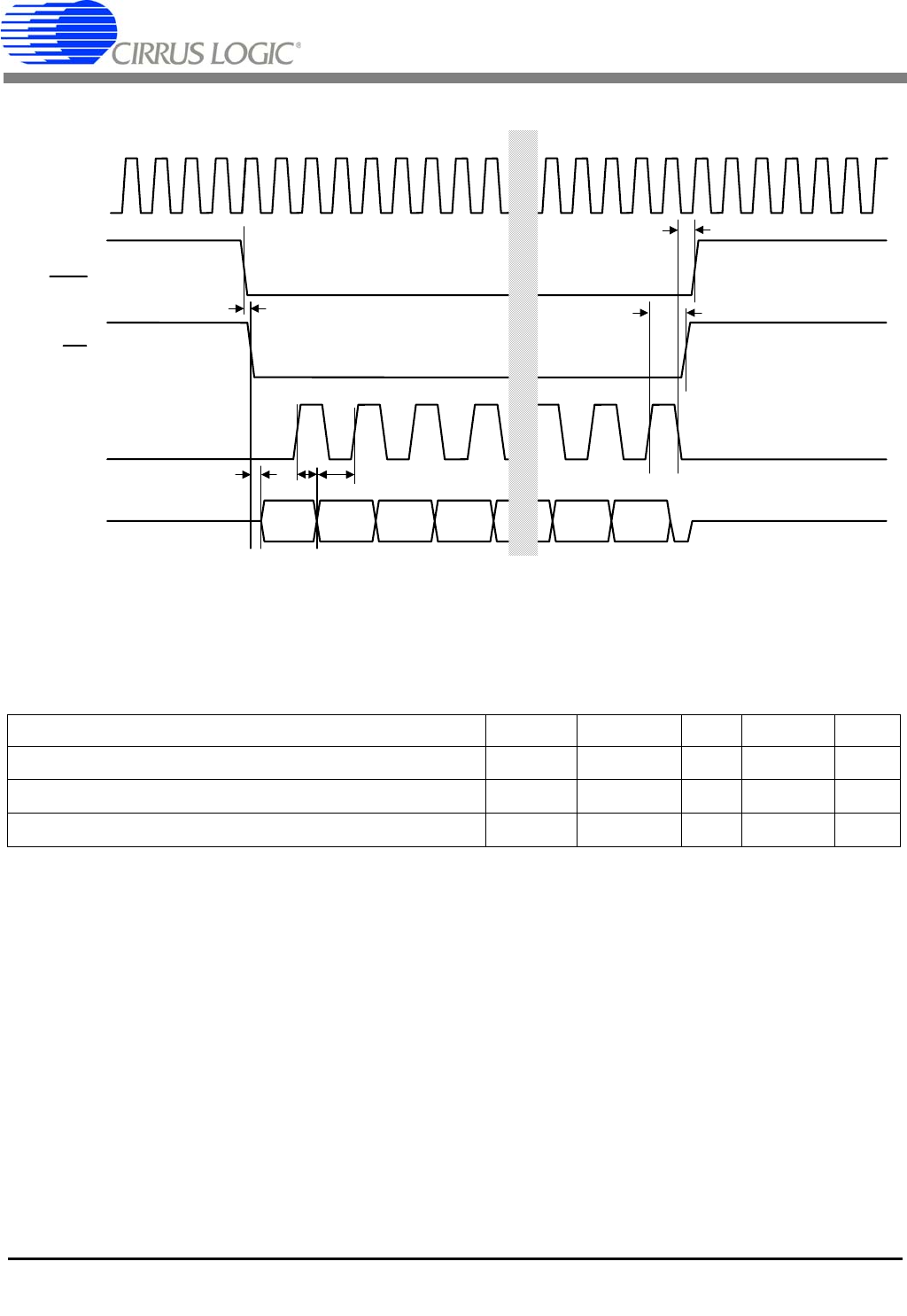
MCLK
SCLK(i)
SDO
CS
RDY
LSBMSB
t
19
t
18
t
20
t
17
t
15
t
21
Figure 4. SEC Mode - Discontinuous SCLK Read Timing (Not to Scale)