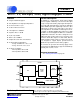
3/25/08 15:11 CS5581 ±2.5 V / 5 V, 200 kSps, 16-bit, High-throughput ∆Σ ADC Features & Description General Description Single-ended Analog Input The CS5581 is a single-channel, 16-bit analog-to-digital converter capable of 200 kSps conversion rate. The input accepts a single-ended analog input signal. On-chip buffers provide high input impedance for both the AIN input and the VREF+ input. This significantly reduces the drive requirements of signal sources and reduces errors due to source impedances.
3/25/08 14:34 CS5581 TABLE OF CONTENTS 1. CHARACTERISTICS AND SPECIFICATIONS . . . . . . . . . . . . . . . . . . . . . . . . . . . . . . . . . . . . 4 ANALOG CHARACTERISTICS . . . . . . . . . . . . . . . . . . . . . . . . . . . . . . . . . . . . . . . . . . . . . . . . 4 SWITCHING CHARACTERISTICS . . . . . . . . . . . . . . . . . . . . . . . . . . . . . . . . . . . . . . . . . . . . . 6 DIGITAL CHARACTERISTICS . . . . . . . . . . . . . . . . . . . . . . . . . . . . . . . . . . . . . . . . . . . . . . . .
/25/08 14:34 CS5581 LIST OF FIGURES Figure 1. SSC Mode - Read Timing, CS remaining low . . . . . . . . . . . . . . . . . . . . . . . . . . . . . . . . . 7 Figure 2. SSC Mode - Read Timing, CS falling after RDY falls . . . . . . . . . . . . . . . . . . . . . . . . . . . 8 Figure 3. SEC Mode - Continuous SCLK Read Timing . . . . . . . . . . . . . . . . . . . . . . . . . . . . . . . . . 9 Figure 4. SEC Mode - Discontinuous SCLK Read Timing . . . . . . . . . . . . . . . . . . . . . . . . . . . . . .
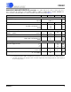
3/25/08 14:34 CS5581 1. CHARACTERISTICS AND SPECIFICATIONS • Min / Max characteristics and specifications are guaranteed over the specified operating conditions. • Typical characteristics and specifications are measured at nominal supply voltages and TA = 25°C. • VLR = 0 V. All voltages measured with respect to 0 V. ANALOG CHARACTERISTICS TA = -40 to +85 °C; V1+ = V2+ = +2.5 V, ±5%; V1- = V2- = -2.5 V, ±5%; VL -VLR = 3.3 V, ±5%; VREF = (VREF+) - (VREF-) = 4.
3/25/08 14:34 CS5581 ANALOG CHARACTERISTICS (CONTINUED) TA = -40 to +85 °C; V1+ = V2+ = +2.5 V, ±5%; V1- = V2- = -2.5 V, ±5%; VL -VLR = 3.3 V, ±5%; VREF = (VREF+) - (VREF-) = 4.096V; MCLK = 16 MHz; SMODE = VL, unless otherwise stated; BUFEN = V1+ unless otherwise stated. Connected per Figure 6.
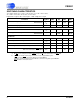
3/25/08 14:34 CS5581 SWITCHING CHARACTERISTICS TA = -40 to +85 °C; V1+ = V2+ = +2.5 V, ±5%; V1- = V2- = -2.5 V, ±5%; VL - VLR = 3.3 V, ±5%, 2.5 V, ±5%, or 1.8 V, ±5% Input levels: Logic 0 = 0V = Low; Logic 1 = VD+ = High; CL = 15 pF. Parameter Master Clock Frequency Internal Oscillator External Clock Symbol Min Typ Max Unit XIN fclk 12 0.5 14 16 16 16.
3/25/08 14:34 CS5581 SWITCHING CHARACTERISTICS (CONTINUED) TA = -40 to +85 °C; V1+ = V2+ = +2.5 V, ±5%; V1- = V2- = -2.5 V, ±5%; VL - VLR = 3.3 V, ±5%, 2.5 V, ±5%, or 1.8 V, ±5% Input levels: Logic 0 = 0V = Low; Logic 1 = VD+ = High; CL = 15 pF.
3/25/08 14:34 CS5581 SWITCHING CHARACTERISTICS (CONTINUED) TA = -40 to +85 °C; V1+ = V2+ = +2.5 V, ±5%; V1- = V2- = -2.5 V, ±5%; VL - VLR = 3.3 V, ±5%, 2.5 V, ±5%, or 1.8 V, ±5% Input levels: Logic 0 = 0V = Low; Logic 1 = VD+ = High; CL = 15 pF.
3/25/08 14:34 CS5581 SWITCHING CHARACTERISTICS (CONTINUED) TA = -40 to +85 °C; V1+ = V2+ = +2.5 V, ±5%; V1- = V2- = -2.5 V, ±5%; VL - VLR = 3.3 V, ±5%, 2.5 V, ±5%, or 1.8 V, ±5% Input levels: Logic 0 = 0V = Low; Logic 1 = VD+ = High; CL = 15 pF.
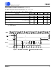
3/25/08 14:34 CS5581 MCLK t21 RDY t15 t20 CS SCLK(i) t17 SDO t18 t19 MSB LSB Figure 4. SEC Mode - Discontinuous SCLK Read Timing (Not to Scale) DIGITAL CHARACTERISTICS TA = TMIN to TMAX; VL = 3.3V, ±5% or VL = 2.5V, ±5% or 1.
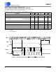
3/25/08 14:34 CS5581 GUARANTEED LOGIC LEVELS TA = -40 to +85 °C; V1+ = V2+ = +2.5 V, ±5%; V1- = V2- = -2.5 V, ±5%; VL - VLR = 3.3 V, ±5%, 2.5 V, ±5%, or 1.8 V, ±5% Input levels: Logic 0 = 0V = Low; Logic 1 = VD+ = High; CL = 15 pF. Guaranteed Limits Parameter Sym VL Min 3.3 1.9 2.5 1.6 1.8 1.2 Typ Max Unit Conditions Logic Inputs Minimum High-level Input Voltage: Maximum Low-level Input Voltage: VIH VIL V 3.3 1.1 2.5 0.95 1.8 0.
3/25/08 14:34 CS5581 RECOMMENDED OPERATING CONDITIONS (VLR = 0V, see Note 16) Parameter Symbol Min Typ Max Unit (Note 16) V1+ V2+ V1V2- V1+ V2V1+ V2- 4.75 4.75 - 5.0 5.0 0 0 5.25 5.25 - V V V V (Note 16) V1+ V2+ V1V2- V1+ V2V1+ V2- +2.375 +2.375 -2.375 -2.375 +2.5 +2.5 -2.5 -2.5 +2.625 +2.625 -2.625 -2.625 V V V V VREF 2.4 4.096 4.2 V Single Analog Supply DC Power Supplies: Dual Analog Supplies DC Power Supplies: Analog Reference Voltage 16. 17.
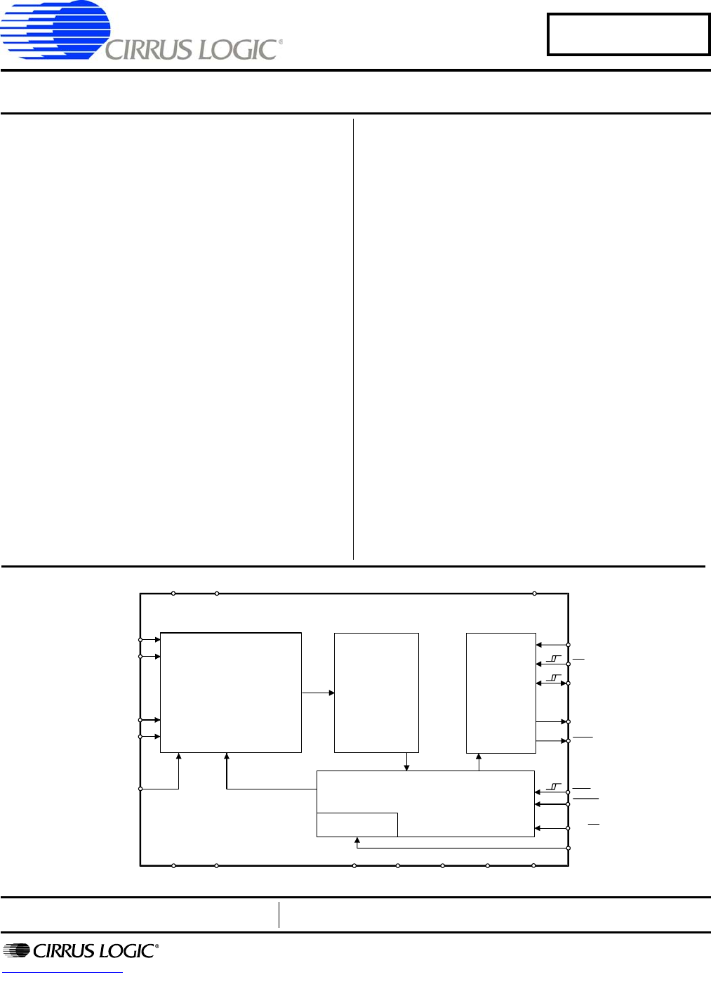
3/25/08 14:34 CS5581 2. OVERVIEW The CS5581 is a 16-bit analog-to-digital converter capable of 200 kSps conversion rate. The analog input accepts a single-ended input with a magnitude of ±VREF / 2 volts. The ADC uses a low-latency digital filter architecture. The filter is designed for fast settling and settles to full accuracy in one conversion. The converter is a serial output device. The serial port can be configured to function as either a master or a slave.
3/25/08 14:34 CS5581 Once a conversion is completed and RDY falls, RDY will return high when all the bits of the data word are emptied from the serial port or if the conversion data is not read and CS is held low, RDY will go high two MCLK cycles before the end of conversion. RDY will fall at the end of the next conversion when new data is put into the port register. See Serial Port on page 24 for information about reading conversion data. Conversion performance can be affected by several factors.
3/25/08 14:34 CS5581 3.3 Voltage Reference The voltage reference for the CS5581 can range from 2.4 volt to 4.2 volts. A 4.096 volt reference is required to achieve the specified signal-to-noise performance. Figure 6 and Figure 7 illustrate the connection of the voltage reference with either a single +5 V analog supply or with ±2.5 V.
3/25/08 14:34 CS5581 3.5 Output Coding Format The reference voltage directly defines the input voltage range in both the unipolar and bipolar configurations. In the unipolar configuration (BP/UP low), the first code transition occurs 0.5 LSB above zero, and the final code transition occurs 1.5 LSBs below VREF. In the bipolar configuration (BP/UP high), the first code transition occurs 0.5 LSB above -VREF and the last transition occurs 1.5 LSBs below +VREF.
3/25/08 14:34 CS5581 3.6 Typical Connection Diagrams The following figure depicts the CS5581 powered from bipolar analog supplies, +2.5 V and - 2.5 V. +2.048 V 0V CS5571 CS5581 -2.048 V 49.9 AIN 150pF 4700pF C0G SMODE 2k CS 5 CS3003 SCLK 5 ACOM SDO RDY (V+) Buffers On BUFEN +2.5 V CONV (V-) Buffers Off BP/UP +4.096 Voltage Reference (NOTE 1) VREF+ 10 µF RST 0.1 µF 50 MCLK VREFTST -2.5 V +3.3 V to +1.8 V +2.5 V V1+ VL 10 0.1 µF V2+ 0.1 µF 0.1 µF 10 V20.
3/25/08 14:34 CS5581 The following figure depicts the CS5581 part powered from a single 5V analog supply and configured for unipolar measurement. 0 V to +2.048 V CS5581 CS5571 49.9 AIN 150pF SMODE 4700pF C0G CS 2k 4 SCLK CS3003 / CS3004 4 ACOM SDO RDY (V+) Buffers On BUFEN +5 V CONV (V-) Buffers Off BP/UP +4.096 Voltage Reference (NOTE 1) VREF+ 10 µF RST 0.1 µF 50 MCLK VREFTST +3.3 V to 1.8 V +5 V V1+ 0.1 µF VL 10 V2+ 0.1 µF 0.1 µF V20.1 µF X7R VLR3 DCR VLR2 V1- VLR NOTES 1.
3/25/08 14:34 CS5581 The following figure depicts the CS5581 part powered from a single 5V analog supply and configured for bipolar measurement, referenced to a common mode voltage of 2.5 V. 0.458 to 4.548 V 49.9 AIN 150pF CS5581 CS5571 CS5581 4700pF C0G 2k SMODE CS3003 / CS3004 Common Mode Voltage (2.5 V Typ.) CS 4 SCLK 49.9 ACOM 150pF 4700pF C0G 4 SDO 2k RDY CS3003 / CS3004 (V+) Buffers On CONV BUFEN +5 V BP/UP (V-) Buffers Off +4.096 Voltage Reference (NOTE 1) VREF+ 10 µF RST 0.
3/25/08 14:34 CS5581 3.7 AIN & VREF Sampling Structures The CS5581 uses on-chip buffers on the AIN and the VREF+ inputs. Buffers provide much higher input impedance and therefore reduce the amount of drive current required from an external source. This helps minimize errors. The Buffer Enable (BUFEN) pin determines if the on-chip buffers are used or not. If the BUFEN pin is connected to the V1+ supply, the buffers will be enabled. If the BUFEN pin is connected to the V1- pin, the buffers are off.
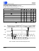
3/25/08 14:34 CS5581 Figures 11 through 16 illustrate the performance of the CS5581 when driven by a 5.55 kHz sine wave at various amplitudes. In each case, the captured data was windowed with a seven-term window function that exhibits 4.3 dB of attenuation before being processed by the FFT. Figure 14 illustrates the converter performance with an input that is 1/10,000 of full scale. This is a signal magnitude of about 6.5 codes, peak to peak.
3/25/08 14:34 CS5581 Figure 16 illustrates the noise floor of the converter from 0.1 Hz to 100 kHz. While the plot does exhibit some 1/f noise at lower frequencies, the noise floor is entirely free of spurious frequency content due to digital activity inside the chip. Figure 17 illustrates a noise histogram of 4096 samples. 0 Shorted Input 2M Samples @ 200 kSps 16 Averages -20 -40 -60 -80 -100 -120 -140 -160 0.1 1 10 100 Frequency (Hz) 1k 10k 100k Figure 16.
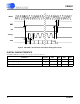
3/25/08 14:34 CS5581 3.9 Digital Filter Characteristics The digital filter is designed for fast settling, therefore it exhibits very little in-band attenuation. The filter attenuation is 0.26347 dB at 100 kHz when sampling at 200 kSps. 0.00 -0.01049 dB -0.05 fs = 200 kSps -0.04206 dB -0.10 -0.09443 dB -0.15 -0.16813 dB -0.20 -0.25 -0.26347 dB -0.30 0 20k 40k 60k 80k 100k Frequency (Hz) Figure 18. CS5581 Spectral Response (DC to fs/2) 0.00 fs = 200 kSps -0.006283 dB -0.002622 dB -0.005 -0.
3/25/08 14:34 CS5581 3.10 Serial Port The serial port on the CS5581 can operate in two different modes: synchronous self clock (SSC) mode & synchronous external clock (SEC) mode. 3.10.1 SSC Mode If the SMODE pin is high (SMODE = VL), the serial port operates in the SSC (Synchronous Self Clock) mode. In the SSC mode the port shifts out conversion data words with SCLK as an output. SCLK is generated inside the converter from MCLK. Data is output from the SDO (Serial Data Output) pin.
3/25/08 14:34 CS5581 3.12 Using the CS5581 in Multiplexing Applications The CS5581 is a delta-sigma A/D converter. Delta-sigma converters use oversampling as means to achieve high signal to noise. This means that once a conversion is started, the converter takes many samples to compute the resulting output word. The analog input for the signal to be converted must remain active during the entire conversion until RDY falls.
3/25/08 14:34 CS5581 At the same time the converter is performing a conversion on a channel from one bank of multiplexers, the second multiplexer bank is used to select the channel for the next conversion. This configuration allows the buffer amplifier for the second multiplexer bank to fully settle while a conversion is being performed on the channel from the first multiplexer bank.
3/25/08 14:34 CS5581 3.13 Synchronizing Multiple Converters Many measurement systems have multiple converters that need to operate synchronously. The converters should all be driven from the same master clock. In this configuration, the converters will convert synchronously if the same CONV signal is used to drive all the converters, and CONV falls on a falling edge of MCLK.
3/26/08 10:50 CS5581 4.
3/25/08 14:34 CS5581 BP/UP – Bipolar/Unipolar Select, Pin 11 The BP/UP pin determines the span and the output coding of the converter. When set high to select BP (bipolar), the input span of the converter is -2.048 volts to +2.048 volts (assuming the voltage reference is 4.096 volts) and output data is coded in two's complement format. When set low to select UP (unipolar), the input span is 0 to +2.048 and the output data is coded in binary format.
3/25/08 14:34 CS5581 SCLK – Serial Clock Input/Output, Pin 23 The SMODE pin determines whether the SCLK signal is an input or an output signal. SCLK determines the rate at which data is clocked out of the SDO pin. If the converter is in SSC mode, the SCLK frequency will be determined by the master clock frequency of the converter (either MCLK or the internal oscillator). In SEC mode, the user determines the SCLK frequency.
3/25/08 14:34 CS5581 5. PACKAGE DIMENSIONS 24L SSOP PACKAGE DRAWING N D E11 A2 E e b2 SIDE VIEW A ∝ A1 L END VIEW SEATING PLANE 1 2 3 TOP VIEW DIM A A1 A2 b D E E1 e L MIN -0.002 0.064 0.009 0.311 0.291 0.197 0.022 0.025 0° ∝ INCHES NOM -0.006 0.068 -0.323 0.307 0.209 0.026 0.03 4° MAX 0.084 0.010 0.074 0.015 0.335 0.323 0.220 0.030 0.041 8° MIN -0.05 1.62 0.22 7.90 7.40 5.00 0.55 0.63 0° MILLIMETERS NOM -0.13 1.73 -8.20 7.80 5.30 0.65 0.75 4° NOTE MAX 2.13 0.25 1.88 0.38 8.50 8.
3/25/08 14:34 CS5581 6. ORDERING INFORMATION Model CS5581-ISZ Linearity Temperature Conversion Time Throughput Package .0008% -40 to +85 °C 5 µs 200 kSps 24-pin SSOP 7. ENVIRONMENTAL, MANUFACTURING, & HANDLING INFORMATION Model Number Peak Reflow Temp MSL Rating* Max Floor Life 260 °C 3 7 Days CS5581-ISZ * MSL (Moisture Sensitivity Level) as specified by IPC/JEDEC J-STD-020. 8. REVISION HISTORY Revision PP1 Date MAR 2008 Changes Preliminary release.