
Manual
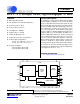
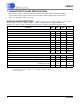
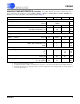

Table Of Contents
- Features & Description
- Table of Contents
- List of Figures
- List of Tables
- 1. Characteristics and Specifications
- Analog Characteristics
- Analog Characteristics (Continued)
- Switching Characteristics
- Switching Characteristics (Continued)
- Switching Characteristics (Continued)
- Switching Characteristics (Continued)
- Digital Characteristics
- Digital Filter Characteristics
- Guaranteed Logic Levels
- Recommended Operating Conditions
- Absolute Maximum Ratings
- 2. Overview
- 3. Theory of Operation
- 3.1 Converter Operation
- 3.2 Clock
- 3.3 Voltage Reference
- 3.4 Analog Input
- 3.5 Output Coding Format
- 3.6 Typical Connection Diagrams
- 3.7 AIN & VREF Sampling Structures
- 3.8 Converter Performance
- 3.9 Digital Filter Characteristics
- 3.10 Serial Port
- 3.11 Power Supplies & Grounding
- 3.12 Using the CS5560 in Multiplexing Applications
- 3.13 Synchronizing Multiple Converters
- 4. Pin Descriptions
- 5. Package Dimensions
- 6. Ordering Information
- 7. Environmental, Manufacturing, & Handling Information
- 8. Revision History
CS5560
DS713PP2 5
5/4/09
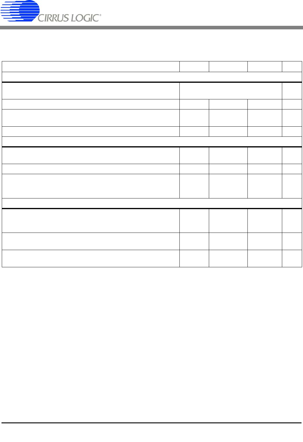
ANALOG CHARACTERISTICS (CONTINUED) T
A
= -40 to +85 °C; V1+ = V2+ = +2.5 V, ±5%; V1- =
V2- = -2.5 V, ±5%; VL -VLR = 3.3 V, ±5%; VREF = (VREF+) - (VREF-) = 4.096V; MCLK = 16 MHz; SMODE = VL.;
BUFEN = V1+ unless otherwise stated. Connected per Figure 6.
4. Measured using an input signal of 1 V DC.
5. For optimum performance, VREF+ should always be less than (V+) - 0.2 volts to prevent saturation of the VREF+ input buffer.
6. Tested with 100 mVP-P on any supply up to 2 kHz. V1+ and V2+ supplies at the same voltage potential, V1- and V2- supplies at
the same voltage potential.
Parameter Min Typ Max Unit
Analog Input
Analog Input Range Unipolar
Bipolar
0 to +VREF
±VREF
V
V
Input Capacitance - 10 - pF
CVF Current (Note 4) AIN Buffer On (BUFEN = V+)
AIN Buffer Off (BUFEN = V-)
-
-
600
130
-
-
nA
μA
Common Mode Rejection Ratio (CMRR) 116 130 - dB
Voltage Reference Input
Voltage Reference Input Range
(VREF+) – (VREF-) (Note 5) 2.4 4.096
4.2
V
Input Capacitance - 10 - pF
CVF Current VREF+ Buffer On (BUFEN = V+)
VREF+ Buffer Off (BUFEN = V-)
VREF-
-
-
-
3
1
1
-
-
-
μA
mA
mA
Power Supplies
DC Power Supply Currents I
V1
I
V2
I
VL
-
-
-
-
-
-
19
1.8
0.6
mA
mA
mA
Power Consumption Normal Operation Buffers On
Buffers Off
-
-
90
60
106
90
mW
mW
Power Supply Rejection (Note 6) V1+ , V2+ Supplies
V1-, V2- Supplies
60
60
70
70
-
-
dB
dB