
Manual


Table Of Contents
- Features & Description
- Table of Contents
- List of Figures
- List of Tables
- 1. Characteristics and Specifications
- Analog Characteristics
- Analog Characteristics (Continued)
- Switching Characteristics
- Switching Characteristics (Continued)
- Switching Characteristics (Continued)
- Switching Characteristics (Continued)
- Digital Characteristics
- Digital Filter Characteristics
- Guaranteed Logic Levels
- Recommended Operating Conditions
- Absolute Maximum Ratings
- 2. Overview
- 3. Theory of Operation
- 3.1 Converter Operation
- 3.2 Clock
- 3.3 Voltage Reference
- 3.4 Analog Input
- 3.5 Output Coding Format
- 3.6 Typical Connection Diagrams
- 3.7 AIN & VREF Sampling Structures
- 3.8 Converter Performance
- 3.9 Digital Filter Characteristics
- 3.10 Serial Port
- 3.11 Power Supplies & Grounding
- 3.12 Using the CS5560 in Multiplexing Applications
- 3.13 Synchronizing Multiple Converters
- 4. Pin Descriptions
- 5. Package Dimensions
- 6. Ordering Information
- 7. Environmental, Manufacturing, & Handling Information
- 8. Revision History
CS5560
26 DS713PP2
5/4/09
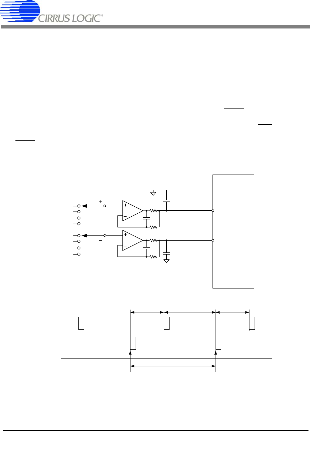
3.12 Using the CS5560 in Multiplexing Applications
The CS5560 is a delta-sigma A/D converter. Delta-sigma converters use oversampling as means to
achieve high signal to noise. This means that once a conversion is started, the converter takes many sam-
ples to compute the resulting output word. The analog input for the signal to be converted must remain
active during the entire conversion until RDY
falls.
The CS5560 can be used in multiplexing applications, but the system timing for changing the multiplexer
channel and for starting a new conversion will depend upon the multiplexer system architecture.
The simplest system is illustrated in Figure 22. Any time the multiplexer is changed, the analog signal
presented to the converter must fully settle. After the signal has settled, the CONV
signal is issued to the
converter to start a conversion. Being a delta-sigma converter, the signal must remain present at the input
of the converter until the conversion is completed. Once the conversion is completed, RDY
falls. At this
time the multiplexer can be changed to the next channel and the data can be read from the serial port.
The CONV
signal should be delayed until after the data is read and until the new analog signal has settled.
In this configuration, the throughput of the converter will be dictated by the settling time of the analog input
circuit and the conversion time of the converter. The conversion data can be read from the serial port after
the multiplexer is changed to the new channel while the analog input signal is settling.
Figure 22. Simple Multiplexing Scheme
A more complex multiplexing scheme can be used to increase the throughput of the converter is illustrated
in Figure 23. In this circuit, two banks of multiplexers are used.
CS556x
AIN+
AIN-
49.9
47pF
4.99k
4700pF
C0G
49.9
47pF
4.99k
4700pF
C0G
CH1+
CH2+
CH3+
CH4+
CH1-
CH2-
CH3-
CH4-
Amplifier
Settling Time
Conversion Time
Amplifier
Settling Time
CH1 CH2
CONV
RDY
Advance
Mux
Throughput