
Manual


Table Of Contents
- Features & Description
- Table of Contents
- List of Figures
- List of Tables
- 1. Characteristics and Specifications
- Analog Characteristics
- Analog Characteristics (Continued)
- Switching Characteristics
- Switching Characteristics (Continued)
- Switching Characteristics (Continued)
- Switching Characteristics (Continued)
- Digital Characteristics
- Digital Filter Characteristics
- Guaranteed Logic Levels
- Recommended Operating Conditions
- Absolute Maximum Ratings
- 2. Overview
- 3. Theory of Operation
- 3.1 Converter Operation
- 3.2 Clock
- 3.3 Voltage Reference
- 3.4 Analog Input
- 3.5 Output Coding Format
- 3.6 Typical Connection Diagrams
- 3.7 AIN & VREF Sampling Structures
- 3.8 Converter Performance
- 3.9 Digital Filter Characteristics
- 3.10 Serial Port
- 3.11 Power Supplies & Grounding
- 3.12 Using the CS5560 in Multiplexing Applications
- 3.13 Synchronizing Multiple Converters
- 4. Pin Descriptions
- 5. Package Dimensions
- 6. Ordering Information
- 7. Environmental, Manufacturing, & Handling Information
- 8. Revision History
CS5560
22 DS713PP2
5/4/09
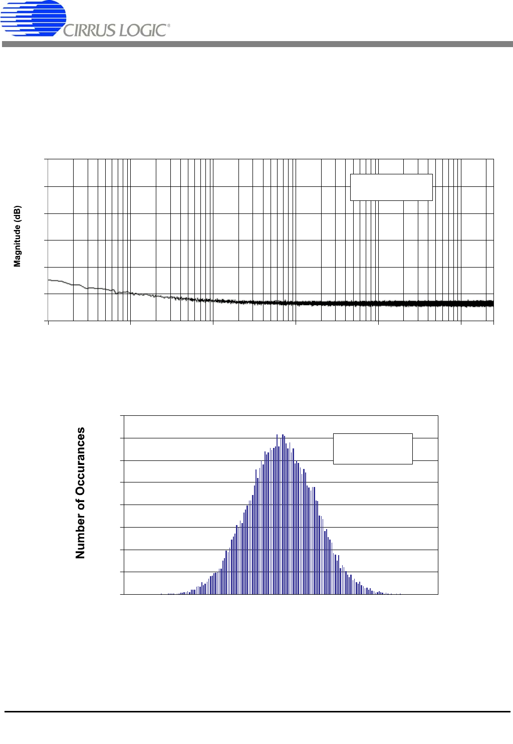
Figure 17 illustrates the noise floor of the converter from 0.1 Hz to 25 kHz. While the plot does exhibit
some 1/f noise at lower frequencies, the noise floor is entirely free of spurious frequency content due to
digital activity inside the chip.
Figure 16 illustrates a noise histogram of 32,768 samples.
-180
-160
-140
-120
-100
-80
-60
0.1 1 10 100 1k 10k
25k
Frequency (Hz)
Shorted Input
1M Samples @ 50 kSps
64 Averages
Figure 17. Spectral Plot of Noise with Shorted Input
0
100
200
300
400
500
600
700
800
Output (Codes)
Std. Dev. = 19.0
Max - Min = 178
Figure 18. Noise Histogram (32k Samples)