
Manual


Table Of Contents
- Features & Description
- Table of Contents
- List of Figures
- List of Tables
- 1. Characteristics and Specifications
- Analog Characteristics
- Analog Characteristics (Continued)
- Switching Characteristics
- Switching Characteristics (Continued)
- Switching Characteristics (Continued)
- Switching Characteristics (Continued)
- Digital Characteristics
- Digital Filter Characteristics
- Guaranteed Logic Levels
- Recommended Operating Conditions
- Absolute Maximum Ratings
- 2. Overview
- 3. Theory of Operation
- 3.1 Converter Operation
- 3.2 Clock
- 3.3 Voltage Reference
- 3.4 Analog Input
- 3.5 Output Coding Format
- 3.6 Typical Connection Diagrams
- 3.7 AIN & VREF Sampling Structures
- 3.8 Converter Performance
- 3.9 Digital Filter Characteristics
- 3.10 Serial Port
- 3.11 Power Supplies & Grounding
- 3.12 Using the CS5560 in Multiplexing Applications
- 3.13 Synchronizing Multiple Converters
- 4. Pin Descriptions
- 5. Package Dimensions
- 6. Ordering Information
- 7. Environmental, Manufacturing, & Handling Information
- 8. Revision History
CS5560
DS713PP2 21
5/4/09
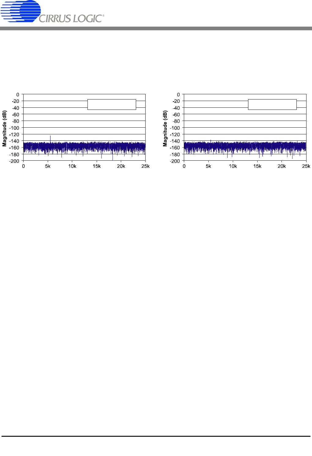
Figure 15 illustrates the device with a small signal 1/1,000,000 of full scale. The signal input for Figure 15
is about 8.2 microvolts peak to peak, or about 17 codes peak to peak. Figure 16 illustrates the converter
with a signal at about 2.6 microvolts peak to peak, or about 5 codes peak to peak. The CS5560 achieves
superb performance with this small signal. And the noise floor exhibits no spurious components due to
digital interference from the on chip logic.
Frequency (Hz)
5.55 kHz, -120 dB
32k Samples @ 50 kSps
Frequency (Hz)
5.55 kHz, -130 dB
32k Samples @ 50 kSps
Figure 15. Spectral Performance, -120 dB Figure 16. Spectral Performance, -130 dB