
Manual
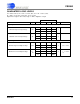
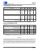

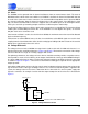
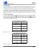


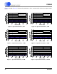
Table Of Contents
- Features & Description
- Table of Contents
- List of Figures
- List of Tables
- 1. Characteristics and Specifications
- Analog Characteristics
- Analog Characteristics (Continued)
- Switching Characteristics
- Switching Characteristics (Continued)
- Switching Characteristics (Continued)
- Switching Characteristics (Continued)
- Digital Characteristics
- Digital Filter Characteristics
- Guaranteed Logic Levels
- Recommended Operating Conditions
- Absolute Maximum Ratings
- 2. Overview
- 3. Theory of Operation
- 3.1 Converter Operation
- 3.2 Clock
- 3.3 Voltage Reference
- 3.4 Analog Input
- 3.5 Output Coding Format
- 3.6 Typical Connection Diagrams
- 3.7 AIN & VREF Sampling Structures
- 3.8 Converter Performance
- 3.9 Digital Filter Characteristics
- 3.10 Serial Port
- 3.11 Power Supplies & Grounding
- 3.12 Using the CS5560 in Multiplexing Applications
- 3.13 Synchronizing Multiple Converters
- 4. Pin Descriptions
- 5. Package Dimensions
- 6. Ordering Information
- 7. Environmental, Manufacturing, & Handling Information
- 8. Revision History
CS5560
16 DS713PP2
5/4/09
3.4 Analog Input
The analog input of the converter is fully differential with a peak-to-peak input of 4.096 volts on each input.
Therefore, the differential, peak-to-peak input is 8.192 volts. This is illustrated in Figure 6 and Figure 7.
These diagrams also illustrate a differential buffer amplifier configuration for driving the CS5560.
The capacitors at the outputs of the amplifiers provide a charge reservoir for the dynamic current from the
A/D inputs while the resistors isolate the dynamic current from the amplifier. The amplifiers can be pow-
ered from higher supplies than those used by the A/D but precautions should be taken to ensure that the
op amp output voltage remains within the power supply limits of the A/D, especially under start-up condi-
tions.
3.5 Output Coding Format
The reference voltage directly defines the input voltage range in both the unipolar and bipolar configura-
tions. In the unipolar configuration (BP/UP
low), the first code transition occurs 0.5 LSB above zero, and
the final code transition occurs 1.5 LSBs below VREF. In the bipolar configuration (BP/UP
high), the first
code transition occurs 0.5 LSB above -VREF and the last transition occurs 1.5 LSBs below +VREF. See
Table 1 for the output coding of the converter.
NOTE: VREF = (VREF+) - (VREF-)
Table 1. Output Coding, Two’s Complement
Bipolar Input Voltage
Two’s
Complement
>(VREF-1.5 LSB) 7F FF FF
VREF-1.5 LSB
7F FF FF
7F FF FE
-0.5 LSB
00 00 00
FF FF FF
-VREF+0.5 LSB
80 00 01
80 00 00
<(-VREF+0.5 LSB) 80 00 00
NOTE: VREF = (VREF+) - (VREF-)
Table 2. Output Coding, Offset Binary
Unipolar Input Voltage
Offset
Binary
>(VREF-1.5 LSB) FF FF FF
VREF-1.5 LSB
FF FF FF
FF FF FE
(VREF/2)-0.5 LSB
80 00 00
7F FF FF
+0.5 LSB
00 00 01
00 00 00
<(+0.5 LSB) 00 00 00