
Instruction Manual
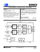

CS5550
6 DS630F1
ANALOG CHARACTERISTICS (Continued)
Notes: 3. The minimum FSCR is limited by the maximum allowed gain register value.
4. All outputs unloaded. All inputs CMOS level.
5.
Definition for PSRR: VREFIN tied to VREFOUT, VA+ = VD+ = 5 V, a 150 mV (zero-to-peak) (60 Hz) sinewave is imposed onto the +5 V DC supply
voltage at VA+ and VD+ pins. The “+” and “-” input pins of both input channels are shorted to AGND. Then the CS5550 is commanded to continuous
conversion acquisition mode, and digital output data is collected for the channel under test. The (zero-to-peak) value of the digital sinusoidal output
signal is determined, and this value is converted into the (zero-to-peak) value of the sinusoidal voltage (measured in mV) that would need to be
applied at the channel’s inputs, in order to cause the same digital sinusoidal output. This voltage is then defined as V
eq. PSRR is then (in dB):
VOLTAGE REFERENCE
Notes: 6. The voltage at VREFOUT is measured across the temperature range. From these measurements the
following formula is used to calculate the VREFOUT Temperature Coefficient:.
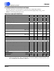
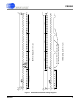
Parameter Symbol Min Typ Max Unit
Dynamic Characteristics
High Rate Filter Output Word Rate OWR - DCLK/1024 - Hz
Input Sampling Rate DCLK = MCLK/K - DCLK/8 - Hz
Full Scale Calibration Range (Note 3) FSCR 25 - 100 %F.S.
High Pass Filter Pole Frequency -3 dB - 0.5 - Hz
Power Supplies
Power Supply Currents (Active State) I
A+
I
D+
(VD+ = 5 V)
I
D+
(VD+ = 3.3 V)
PSCA
PSCD
PSCD
-
-
-
1.3
2.9
1.7
-
-
-
mA
mA
mA
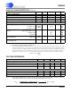
Power Consumption Active State (VD+ = 5 V)
(Note 4) Active State (VD+ = 3.3 V)
Stand-by State
Sleep State
PC -
-
-
-
21
11.6
6.75
10
30
-
-
-
mW
mW
mW
µW
Power Supply Rejection Ratio (AIN1
±) (Gain = 10)
(50, 60 Hz)(Note 5) (Gain = 50)
PSRR
1
PSRR
1
56
70
-
-
-
-
dB
dB
Power Supply Rejection Ratio (AIN2
±) (Gain = 50)
(50, 60 Hz)(Note 5)
PSRR
2
-55-dB
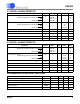
Parameter Symbol Min Typ Max Unit
Reference Output
Output Voltage REFOUT 2.4 - 2.6 V
Temperature Coefficient (Note 6) TC - 25 60 ppm/°C
Load Regulation (Output Current 1 µA Source or Sink) ∆V
R
-610mV
Reference Input
Input Voltage Range VREFIN 2.4 2.5 2.6 V
Input Capacitance - 4 - pF
Input CVF Current - 25 - nA
PSRR 20
150
V
eq
---------
⎩⎭
⎨⎬
⎧⎫
log⋅=
(VREFOUTMAX - VREFOUTMIN)
VREFOUT
AVG
(
(
1
T
A
MAX
- T
A
MIN
(
(
1.0 x 10
(
(
6
TC
VREF
=