
Instruction Manual

CS5550
4 DS630F1
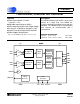
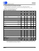
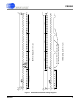
1. PIN DESCRIPTION
VREFIN 12Voltage Reference Input
VREFOUT 11Voltage Reference Output
AIN2- 10Differential Analog Input
AIN2+ 9Differential Analog Input
TSTO 8Test Output
CS 7Chip Select
SDO 6Serial Data Ouput
SCLK 5Serial Clock
DGND 4Digital Ground
VD+ 3Positive Power Supply
CPUCLK 2CPU Clock Output
XOUT 1Crystal Out
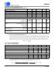
AGND13 Analog Ground
VA+14 Positive Analog Supply
AIN1-15 Differential Analog Input
AIN1+16 Differential Analog Input
TSTO17 Test Output
TSTO18 Test Output
RESET19 Reset
INT20 Interrupt
TSTO21 Test Output
TSTO22 Test Output
SDI23 Serial Data Input
XIN24 Crystal In
Clock Generator
Crystal Out
Crystal In
1,24 XOUT, XIN - A gate inside the chip is connected to these pins and can be used with a
crystal to provide the system clock for the device. Alternatively, an external (CMOS
compatible) clock can be supplied into XIN pin to provide the system clock for the device.
CPU Clock Output
2 CPUCLK - Output of on-chip oscillator which can drive one standard CMOS load.
Control Pins and Serial Data I/O
Serial Clock Input
5 SCLK - A clock signal on this pin determines the input and output rate of the data for the
SDI and SDO pins respectively. The SCLK pin will recognize clocks only when CS is low.
Serial Data Output
6 SDO -The serial data port output pin. Its output is in a high impedance state when CS is
high.
Chip Select
7 CS - When low, the port will recognize SCLK. An active high on this pin forces the SDO
pin to a high impedance state. CS should be changed when SCLK is low.
Reset
19 RESET - When reset is taken low, all internal registers are set to their default states.
Interrupt
20 INT - When INT goes low it signals that an enabled event has occurred.
Serial Data Input
23 SDI - The serial data port input pin. Data will be input at a rate determined by SCLK.
Measurement and Reference Input
Differential
Analog Inputs
9,10,15,16 AIN1+, AIN1-, AIN2+, AIN2- - Differential analog input pins.
Voltage
Reference Output
11 VREFOUT - The on-chip voltage reference output. The voltage reference has a nominal
magnitude of 2.5 V and is referenced to the AGND pin on the converter.
Voltage
Reference Input
12 VREFIN - The input establishes the voltage reference for the on-chip modulator.
Power Supply Connections
Positive
Digital Supply
3 VD+ - The positive digital supply relative to DGND.
Digital Ground
4,9,10 DGND - The common-mode potential of digital ground must be equal to or above the
common-mode potential of AGND.
Positive
Analog Supply
14 VA+ - The positive analog supply relative to AGND.
Analog Ground 13
AGND - The analog ground pin must be at the lowest potential.
Test Output
8,17,18,21,22 TSTO - These pins are used for factory testing and must be left floating.