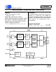
CS5550 Two-channel, Low-cost A/D Converter Features Description z Power The CS5550 combines two ∆Σ ADCs and a serial interface on a single chip. The CS5550 has on-chip functionality to facilitate offset and gain calibration. The CS5550 features a bi-directional serial interface for communication with a microcontroller. Consumption <12 mW - with VD+ = 3.3 V Input Range on AIN1± z GND-referenced Signals with Single Supply z On-chip 2.
CS5550 TABLE OF CONTENTS 1. PIN DESCRIPTION ................................................................................................................... 4 2. CHARACTERISTICS/SPECIFICATIONS ................................................................................. 5 ANALOG CHARACTERISTICS ................................................................................................ 5 VOLTAGE REFERENCE.............................................................................................
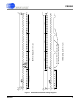
CS5550 LIST OF FIGURES Figure 1. CS5550 Read and Write Timing Diagrams...................................................................... 9 Figure 2. Oscillator Connection..................................................................................................... 11 Figure 3. System Calibration of Gain. ........................................................................................... 12 Figure 4. System Calibration of Offset. ............................................................
CS5550 1.
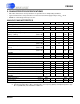
CS5550 2. CHARACTERISTICS/SPECIFICATIONS • Min / Max characteristics and specifications are guaranteed over all Operating Conditions. • Typical characteristics and specifications are measured at nominal supply voltages and TA = 25°C. • DGND = 0 V. All voltages with respect to 0 V. ANALOG CHARACTERISTICS Parameter Symbol Min Typ Max Unit CMRR 80 - - dB - 5 - nV/°C AIN1 0 0 - 500 100 mVP-P mVP-P THD1 80 - - dB -0.
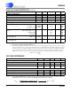
CS5550 ANALOG CHARACTERISTICS (Continued) Parameter Symbol Min Typ Max Unit OWR - DCLK/1024 - Hz - DCLK/8 - Hz 25 - 100 %F.S. - 0.5 - Hz PSCA PSCD PSCD - 1.3 2.9 1.7 - mA mA mA PC - 21 11.6 6.
CS5550 5 V DIGITAL CHARACTERISTICS Parameter Symbol Min Typ Max Unit High-Level Input Voltage All Pins Except XIN and SCLK and RESET XIN SCLK and RESET VIH 0.6 VD+ (VD+) - 0.5 0.8 VD+ - - V V V Low-Level Input Voltage All Pins Except XIN and SCLK and RESET XIN SCLK and RESET VIL - - 0.8 1.5 0.2 VD+ V V V High-Level Output Voltage Iout = +5 mA VOH (VD+) - 1.0 - - V Low-Level Output Voltage Iout = -5 mA VOL - - 0.
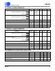
CS5550 SWITCHING CHARACTERISTICS 50 50 Max 5 60 60 1.0 100 1.
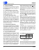
DS630F1 SDI SCLK SDO CS SDI SCLK CS t 7 t3 MSB MSB MSB - 1 MSB - 1 t2 t2 Command Time 8 SCLKs t1 Command Time 8 SCLKs t1 LSB LSB MSB t MSB 8 4 MSB - 1 MSB - 1 t 5 MSB MSB - 1 High Byte LSB MSB MSB - 1 SDI Write Timing (Not to Scale) High Byte LSB Mid Byte Mid Byte SDO Read Timing (Not to Scale) Must strobe "SYNC0" command on SDI when reading each byte of data from SDO.
CS5550 2.1 Theory of Operation The analog signals at the analog inputs are subject to the gains of the input PGAs. These signals are then sampled by the delta-sigma modulators at a rate of (MCLK/K) / 8. 2.1.1 High-Rate Digital Low-Pass Filters The data is then low-pass filtered, to remove high-frequency noise from the modulator output. The high rate filters on both channels are implemented as fixed Sinc3 filters. 2.1.
CS5550 This linearity is guaranteed for all available full-scale input voltage ranges. device. If higher accuracy/stability is required, an external reference can be used. Note that until the CS5550 is calibrated (see Calibration) the accuracy of the CS5550 is not guaranteed to within ±0.1%. But the linearity of any given sample of CS5550, before calibration, will be within ±0.
CS5550 3.4 Calibration 3.4.1 Overview of Calibration Process The CS5550 offers digital calibration for offset and gain. Since both channels have separate offset and gain registers associated with them, system offset or system gain can be performed on either channel without the calibration results from one channel affecting the other. maximum instantaneous voltage level that needs to be measured across the inputs (including the maximum over-range level that must be accurately measured).
CS5550 is added to the signal path to nullify the DC offset in the system. 3.4.5.2 Gain Calibration Sequence Based on the level of the positive DC calibration voltage applied across the “+’ and “-” inputs, the CS5550 determines the Gain Register value by averaging the Digital Output Register’s output signal values over one computation cycle (N samples) and then dividing this average into 1.
CS5550 pulse-low, the duration of the INT pulse will be at least one DCLK cycle (DCLK = MCLK / K). 3.6 PCB Layout pins of the device connected to the analog plane. Place the analog-digital plane split immediately adjacent to the digital portion of the chip.
CS5550 4. SERIAL PORT OVERVIEW The CS5550's serial port incorporates a state machine with transmit/receive buffers. The state machine interprets 8-bit command words on the rising edge of SCLK. Upon decoding of the command word, the state machine performs the requested command or prepares for a data transfer of the addressed register. Request for a read requires an internal register transfer to the transmit buffer, while a write waits until the completion of 24 SCLKs before performing a transfer.
CS5550 4.1.4 Power-Up/Halt B7 1 B6 0 B5 1 B4 0 B3 0 B2 0 B1 0 B0 0 If the device is powered-down, this command will power-up the device. When powered-on, no computations will be running. If the part is already powered-on, all computations will be halted. 4.1.5 Power-Down and Software Reset B7 1 B6 0 B5 0 B4 S1 B3 S0 B2 0 B1 0 B0 0 The device has two power-down states to conserve power.
CS5550 4.1.7 Register Read/Write B7 0 B6 W/R B5 RA4 B4 RA3 B3 RA2 B2 RA1 B1 RA0 B0 0 The Read/Write command informs the state machine that a register access is required. During a read operation, the addressed register is loaded into the device’s output buffer and clocked out by SCLK. During a write operation, the data is clocked into the input buffer and, and all 24 bits are transferred to the addressed register on the 24th SCLK.
CS5550 4.2 Serial Port Interface The CS5550’s serial interface consists of four control lines, which have the following pin-names: CS, SDI, SDO, and SCLK. CS, Chip Select, is the control line which enables access to the serial port. If the CS pin is tied to logic 0, the port can function as a three wire interface. SDI, Serial Data In, is the data signal used to transfer data to the converters. SDO, Serial Data Out, is the data signal used to transfer output data from the converters.
CS5550 as well as the other defined power states of the CS5550, are described in Section 4.6). Refer to Section 5 of the data sheet to see the default register values for any particular device register. 4.5 Serial Port Initialization It is possible for the serial interface to become unsynchronized, with respect to the SCLK input.
CS5550 5. REGISTER DESCRIPTION 1. “Default**” => bit status after power-on or reset 2. Any bit not labeled is Reserved. A zero should always be used when writing to one of these bits. 5.1 Configuration Register Address: 0 23 22 21 20 19 18 17 16 gain 15 14 13 12 IMODE 11 IINV 10 9 8 7 6 2HPF 5 1HPF 4 iCPU 3 K3 2 K2 1 K1 0 K0 Default** = 0x000001 gain Sets the gain of the AIN1 PGA 0 = gain is 10 1 = gain is 50 [IMODE IINV] Soft interrupt configuration bits.
CS5550 5.2 Offset Registers Address: 1 (Offset Register - AIN1) 3 (Offset Register - AIN2) MSB -(20) LSB 2-1 2-2 2-3 2-4 2-5 2-6 2-7 ..... 2-17 2-18 2-19 2-20 2-21 2-22 2-23 Default** = 0.000 The Offset Registers are initialized to zero on reset, allowing the device to function and perform measurements. The register is loaded after one computation cycle with the offset when the proper input is applied and the Calibration Command is received.
CS5550 5.5 OUT1 and OUT2 Output Registers Address: 7 (AIN1 Output Register) 8 (AIN2 Output Register) MSB LSB -(20) 2-1 2-2 2-3 2-4 2-5 2-6 2-7 2-17 ..... 2-18 2-19 2-20 2-21 2-22 2-23 These signed registers contain the last value of the measured results of AIN1 and AIN2. The results will be within the range of -1.0 ≤ AIN1,AIN2 < 1.0. The value is represented in two's complement notation, with the binary point place to the right of the MSB (MSB has a negative weighting).
CS5550 small to fit in the AIN Output Register. CRDY Conversion Ready. Indicates a new conversion is ready. OD1, OD2 Modulator oscillation detect. Set when the modulator oscillates due to an input above Full Scale. Note that the level at which the modulator oscillates is significantly higher than the Input Voltage Range. FOR1, FOR2 FILT out of range. Set when the calibrated voltage value is too large for the FILT register. IC Invalid Command. Normally logic 1.
CS5550 6. PACKAGE DIMENSIONS 24L SSOP PACKAGE DRAWING N D E11 A2 E e b2 SIDE VIEW A ∝ A1 L END VIEW SEATING PLANE 1 2 3 TOP VIEW DIM A A1 A2 b D E E1 e L ∝ MIN -0.002 0.064 0.009 0.311 0.291 0.197 0.022 0.025 0° INCHES NOM -0.006 0.068 -0.323 0.307 0.209 0.026 0.03 4° MAX 0.084 0.010 0.074 0.015 0.335 0.323 0.220 0.030 0.041 8° MIN -0.05 1.62 0.22 7.90 7.40 5.00 0.55 0.63 0° MILLIMETERS NOM -0.13 1.73 -8.20 7.80 5.30 0.65 0.75 4° NOTE MAX 2.13 0.25 1.88 0.38 8.50 8.20 5.60 0.75 1.