
Manual

CS5531/32/33/34-AS
10 DS289F5
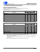
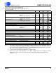
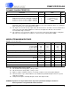
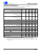
SWITCHING CHARACTERISTICS
(VA+ = 2.5 V or 5 V ±5%; VA- = -2.5V±5% or 0 V; VD+ = 3.0 V ±10% or 5 V ±5%;DGND = 0 V;
Levels: Logic 0 = 0 V, Logic 1 = VD+; C
L
= 50 pF; See Figures 1 and 2.)
Notes: 26. Device parameters are specified with a 4.9152 MHz clock.
27. Specified using 10% and 90% points on waveform of interest. Output loaded with 50 pF.
28. Oscillator start-up time varies with crystal parameters. This specification does not apply when using an
external clock source.
Parameter Symbol Min Typ Max Unit
Master Clock Frequency (Note 26)
External Clock or Crystal Oscillator
MCLK
1 4.9152 5 MHz
Master Clock Duty Cycle 40 - 60 %
Rise Times (Note 27)
Any Digital Input Except SCLK
SCLK
Any Digital Output
t
rise
-
-
-
-
-
50
1.0
100
-
µs
µs
ns
Fall Times (Note 27)
Any Digital Input Except SCLK
SCLK
Any Digital Output
t
fall
-
-
-
-
-
50
1.0
100
-
µs
µs
ns
Start-up
Oscillator Start-up Time XTAL = 4.9152 MHz (Note 28) t
ost
-20-ms
Serial Port Timing
Serial Clock Frequency SCLK 0 - 2 MHz
Serial Clock Pulse Width High
Pulse Width Low
t
1
t
2
250
250
-
-
-
-
ns
ns
SDI Write Timing
CS
Enable to Valid Latch Clock t
3
50 - - ns
Data Set-up Time prior to SCLK rising t
4
50 - - ns
Data Hold Time After SCLK Rising t
5
100 - - ns
SCLK Falling Prior to CS
Disable t
6
100 - - ns
SDO Read Timing
CS
to Data Valid t
7
--150ns
SCLK Falling to New Data Bit t
8
--150ns
CS
Rising to SDO Hi-Z t
9
--150ns