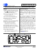
CS5531/32/33/34-AS 16-bit and 24-bit ADCs with Ultra-low-noise PGIA Features General Description Chopper-stabilized The CS5531/32/33/34 are highly integrated ∆Σ Analogto-Digital Converters (ADCs) which use charge-balance techniques to achieve 16-bit (CS5531/33) and 24-bit (CS5532/34) performance. The ADCs are optimized for measuring low-level unipolar or bipolar signals in weigh scale, process control, scientific, and medical applications.
CS5531/32/33/34-AS TABLE OF CONTENTS 1. CHARACTERISTICS AND SPECIFICATIONS ..........................................................4 ANALOG CHARACTERISTICS..........................................................................4 TYPICAL RMS NOISE (NV), CS5531/32/33/34 .................................................7 TYPICAL NOISE-FREE RESOLUTION(BITS), CS5532/34 ...............................7 5 V DIGITAL CHARACTERISTICS ....................................................................
CS5531/32/33/34-AS LIST OF FIGURES Figure 1. SDI Write Timing (Not to Scale)............................................................................... 11 Figure 2. SDO Read Timing (Not to Scale)............................................................................. 11 Figure 3. Multiplexer Configuration ......................................................................................... 12 Figure 4. Input models for AIN+ and AIN- pins .........................................................
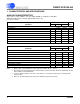
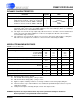
CS5531/32/33/34-AS 1. CHARACTERISTICS AND SPECIFICATIONS ANALOG CHARACTERISTICS (VA+, VD+ = 5 V ±5%; VREF+ = 5 V; VA-, VREF-, DGND = 0 V; MCLK = 4.9152 MHz; OWR (Output Word Rate) = 60 Sps; Bipolar Mode; Gain = 32) (See Notes 1 and 2.) CS5531/CS5533 Parameter Accuracy Linearity Error No Missing Codes Bipolar Offset Unipolar Offset Offset Drift Bipolar Full-scale Error Unipolar Full-scale Error Full-scale Drift (Notes 3 and 4) (Note 4) Min Typ Max Unit 16 - ±0.0015 ±1 ±0.
CS5531/32/33/34-AS ANALOG CHARACTERISTICS (Continued) (See Notes 1 and 2.) Parameter Min Typ Analog Input Common Mode + Signal on AIN+ or AIN-Bipolar/Unipolar Mode Gain = 1 VAGain = 2, 4, 8, 16, 32, 64 (Note 5) VA- + 0.
CS5531/32/33/34-AS ANALOG CHARACTERISTICS (Continued) (See Notes 1 and 2.) Parameter Min Typ Max Unit - 6 0.6 8 1 mA mA - 35 5 500 45 - mW mW µW - 115 115 - dB dB Power Supplies DC Power Supply Currents (Normal Mode) Power Consumption Normal Mode Standby Sleep Power Supply Rejection IA+, IAID+ (Notes 8 and 9) (Note 10) dc Positive Supplies dc Negative Supply 8. All outputs unloaded. All input CMOS levels. 9. Power is specified when the instrumentation amplifier (Gain ≥ 2) is on.
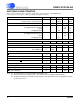
CS5531/32/33/34-AS TYPICAL RMS NOISE (nV), CS5531/32/33/34 (See notes 11, 12 and 13) Output Word -3 dB Filter Rate (Sps) Frequency (Hz) 7.5 1.94 15 3.88 30 7.75 60 15.
CS5531/32/33/34-AS 5 V DIGITAL CHARACTERISTICS (VA+, VD+ = 5 V ±5%; VA-, DGND = 0 V; See Notes 2 and 16.) Parameter Symbol Min Typ Max Unit High-level Input Voltage All Pins Except SCLK SCLK VIH 0.6 VD+ (VD+) - 0.45 - VD+ VD+ V Low-level Input Voltage All Pins Except SCLK SCLK VIL 0.0 0.0 - 0.8 0.6 V High-level Output Voltage A0 and A1, Iout = -1.0 mA SDO, Iout = -5.0 mA VOH (VA+) - 1.0 (VD+) - 1.0 - - V Low-level Output Voltage A0 and A1, Iout = 1.0 mA SDO, Iout = 5.
CS5531/32/33/34-AS DYNAMIC CHARACTERISTICS Parameter Symbol Ratio Unit Modulator Sampling Rate fs MCLK/16 Sps Filter Settling Time to 1/2 LSB (Full-scale Step Input) Single Conversion mode (Notes 17, 18, and 19) Continuous Conversion mode, OWR < 3200 Sps Continuous Conversion mode, OWR ≥ 3200 Sps ts ts ts 1/OWRSC 5/OWRsinc5 + 3/OWR 5/OWR s s s 17. The ADCs use a Sinc5 filter for the 3200 Sps and 3840 Sps output word rate (OWR) and a Sinc5 filter followed by a Sinc3 filter for the other OWRs.
CS5531/32/33/34-AS SWITCHING CHARACTERISTICS (VA+ = 2.5 V or 5 V ±5%; VA- = -2.5V±5% or 0 V; VD+ = 3.0 V ±10% or 5 V ±5%;DGND = 0 V; Levels: Logic 0 = 0 V, Logic 1 = VD+; CL = 50 pF; See Figures 1 and 2.) Parameter Min Typ Max Unit 1 4.9152 5 MHz 40 - 60 % - 50 1.0 100 - µs µs ns - 50 1.
CS5531/32/33/34-AS CS t3 SDI M SB M S B -1 t4 LSB t5 t1 t6 SC LK t2 Figure 1. SDI Write Timing (Not to Scale) CS t7 SDO t9 MSB M S B -1 LS B t2 t8 SC LK t1 Figure 2.
CS5531/32/33/34-AS 2. GENERAL DESCRIPTION The CS5531/32/33/34 are highly integrated ∆Σ Analog-to-Digital Converters (ADCs) which use charge-balance techniques to achieve 16-bit (CS5531/33) and 24-bit (CS5532/34) performance. The ADCs are optimized for measuring low-level unipolar or bipolar signals in weigh scale, process control, scientific, and medical applications.
CS5531/32/33/34-AS instrumentation amplifier is typically 1200 pA over -40°C to +85°C (MCLK=4.9152 MHz). The common-mode plus signal range of the instrumentation amplifier is (VA-) + 0.7 V to (VA+) 1.7 V. Figure 4 illustrates the input models for the amplifiers. The dynamic input current for each of the pins can be determined from the models shown. Gain = 2, 4, 8, 16, 32, 64 AIN C = 3 .
CS5531/32/33/34-AS An offset DAC was not included in the CS553X family because the high dynamic range of the converter eliminates the need for one. The offset register can be manipulated by the user to mimic the function of a DAC if desired. 2.2. Overview of ADC Register Structure and Operating Modes The CS5531/32/33/34 ADCs have an on-chip controller, which includes a number of user-accessible registers.
CS5531/32/33/34-AS instruct the converter to perform single or multiple conversions or calibrations with the converter in the mode defined by one of these Setups. Using the single conversion mode, an 8-bit command word can be written into the serial port. The command includes pointer bits which ‘point’ to a 16-bit command in one of the Channel Setup Registers which is to be executed. The 16-bit Setups can be programmed to perform a conversion on any of the input channels of the converter.
CS5531/32/33/34-AS caused an operational issue for customers because their start-up sequence includes writing a word (with RS=0) into the configuration register after performing a reset. The change in the reset sequence to include writing the RS bit back to 0 insures the clearing of the RS bit in the event that a user does not write into the configuration register after the RS bit has been set. The RV bit in the Configuration Register is set to indicate a valid reset has occurred.
CS5531/32/33/34-AS 2.2.2. Command Register Quick Reference D7(MSB) D6 D5 D4 D3 D2 D1 D0 0 ARA CS1 CS0 R/W RSB2 RSB1 RSB0 BIT NAME D7 Command Bit, C VALUE FUNCTION 0 1 Must be logic 0 for these commands. These commands are invalid if this bit is logic 1. D6 Access Registers as Arrays, ARA 0 1 Ignore this function. Access the respective registers, offset, gain, or channel-setup, as an array of registers. The particular registers accessed are determined by the RS bits.
CS5531/32/33/34-AS 2.2.3. Command Register Descriptions READ/WRITE ALL OFFSET CALIBRATION REGISTERS D7(MSB) 0 Function: D6 1 D5 0 D4 0 D3 R/W D2 0 D1 0 D0 1 D1 1 D0 0 D1 0 D0 1 These commands are used to access the offset registers as arrays. R/W (Read/Write) 0 Write to selected registers. 1 Read from selected registers. READ/WRITE ALL GAIN CALIBRATION REGISTERS D7(MSB) 0 Function: D6 1 D5 0 D4 0 D3 R/W D2 0 These commands are used to access the gain registers as arrays.
CS5531/32/33/34-AS READ/WRITE INDIVIDUAL GAIN REGISTER D7(MSB) 0 Function: D6 0 D5 CS1 D4 CS0 D3 R/W D2 0 D1 1 D0 0 These commands are used to access each gain register separately. CS1 - CS0 decode the registers accessed. R/W (Read/Write) 0 Write to selected register. 1 Read from selected register.
CS5531/32/33/34-AS PERFORM CONVERSION D7(MSB) 1 Function: D6 MC D5 CSRP2 D4 CSRP1 D3 CSRP0 D2 0 D1 0 D0 0 These commands instruct the ADC to perform either a single, fully-settled conversion or continuous conversions on the physical input channel pointed to by the pointer bits (CSRP2 CRSP0) in the channel-setup register. MC (Multiple Conversions) 0 Perform a single conversion. 1 Perform continuous conversions.
CS5531/32/33/34-AS PERFORM CALIBRATION D7(MSB) 1 Function: D6 0 D5 CSRP2 D4 CSRP1 D3 CSRP0 D2 CC2 D1 CC1 D0 CC0 These commands instruct the ADC to perform a calibration on the physical input channel selected by the setup register which is chosen by the command byte pointer bits (CSRP2 CSRP0).
CS5531/32/33/34-AS 2.2.4. Serial Port Interface The CS5531/32/33/34’s serial interface consists of four control lines: CS, SDI, SDO, SCLK. Figure 7 details the command and data word timing. CS, Chip Select, is the control line which enables access to the serial port. If the CS pin is tied low, the port can function as a three-wire interface. SDI, Serial Data In, is the data signal used to transfer data to the converters.
CS5531/32/33/34-AS 2.2.5. Reading/Writing On-Chip Registers 2.3.1. Power Consumption The CS5531/32/33/34’s offset, gain, configuration, and channel-setup registers are readable and writable while the conversion data register is read only. The CS5531/32/33/34 accommodate three power consumption modes: normal, standby, and sleep. The default mode, “normal mode”, is entered after power is applied. In this mode, the CS5531/32/33/34 devices typically consume 35 mW.
CS5531/32/33/34-AS ter is read. The on-chip registers are initialized to the following default states: Configuration Register: Offset Registers: Gain Registers: Channel Setup Registers: 00000000(H) 00000000(H) 01000000(H) 00000000(H) After reset, the RS bit should be written back to logic 0 to complete the reset cycle. The ADC will return to the command mode where it waits for a valid command. Also, the RS bit is the only bit in the configuration register that can be set when initiating a reset (i.e.
CS5531/32/33/34-AS φ1 Fine φ1 Fine φ2 Coarse VREF C = 14pF Vos ≤ 8 mV in = fVos C MCLK 16 VRS = 1; 1 V ≤ VREF ≤ 2.5 V f= Figure 9. Input Reference Model when VRS = 1 from VA+ and VA-. Their output voltage will be limited to the VA+ voltage for a logic 1 and VAfor a logic 0. 2.3.7. Offset and Gain Select The Offset and Gain Select bit (OGS) is used to select the source of the calibration registers to use when performing conversions and calibrations.
CS5531/32/33/34-AS 2.3.9. Configuration Register Descriptions D31(MSB) D30 PSS PDW D15 D14 NU NU D29 RS D13 NU D28 RV D12 NU D27 IS D11 NU D26 GB D10 NU D25 VRS D9 NU D24 A1 D8 NU D23 A0 D7 NU D22 OLS D6 NU D21 NU D5 NU D20 OGS D4 NU D19 FRS D3 NU D18 NU D2 NU D17 NU D1 NU D16 NU D0 NU PSS (Power Save Select)[31] 0 Standby Mode (Oscillator active, allows quick power-up). 1 Sleep Mode (Oscillator inactive). PDW (Power Down Mode)[30] 0 Normal Mode 1 Activate the power save select mode.
CS5531/32/33/34-AS Filter Rate Select, FRS[19] 0 Use the default output word rates. 1 Scale all output word rates and their corresponding filter characteristics by a factor of 5/6. NU (Not Used)[18:0] 0 Must always be logic 0. Reserved for future upgrades. 2.4. Setting up the CSRs for a Measurement The CS5531/32/33/34 have four channel-setup registers (CSRs).
CS5531/32/33/34-AS 2.4.1.
CS5531/32/33/34-AS U/B (Unipolar / Bipolar) [22] [6] 0 Select Bipolar mode. 1 Select Unipolar mode. OL1-OL0 (Output Latch Bits) [21:20] [5:4] The latch bits will be set to the logic state of these bits upon command word execution when the output latch select bit (OLS) in the configuration register is logic 0. Note that the logic outputs on the chip are powered from VA+ and VA-.
CS5531/32/33/34-AS 2.5. Calibration Calibration is used to set the zero and gain slope of the ADC’s transfer function. The CS5531/32/33/34 offer both self-calibration and system calibration. Note: After the ADCs are reset, they are functional and can perform measurements without being calibrated (remember that the VRS bit in the configuration register must be properly configured). In this case, the converter will utilize the initialized values of the on-chip registers (Gain = 1.0, Offset = 0.
CS5531/32/33/34-AS 2.5.4. Performing Calibrations To perform a calibration, the user must send a command byte with its MSB = 1, its pointer bits (CSRP2-CSRP0) set to address the desired Setup to calibrate, and the appropriate calibration bits (CC2CC0) set to choose the type of calibration to be performed.
CS5531/32/33/34-AS 2.5.6. System Calibration For the system calibration functions, the user must supply the converter’s calibration signals which represent ground and full scale. When a system offset calibration is performed, a ground-referenced signal must be applied to the converters. Figure 13 illustrates system offset calibration. As shown in Figure 14, the user must input a signal representing the positive full-scale point to perform a system gain calibration.
CS5531/32/33/34-AS crocontroller and the ADC, and may prematurely halt the calibration cycle. For maximum accuracy, calibrations should be performed for both offset and gain (selected by changing the G2-G0 bits of the channel-setup registers). Note that only one gain range can be calibrated per physical channel when the OGS bit in the Configuration Register is set to ‘0’.
CS5531/32/33/34-AS rial port returns to the command mode, where it waits for a new command to be issued. The single conversion mode will take longer than conversions performed in the continuous conversion mode. The number of clock cycles a single conversion takes for each Output Word Rate (OWR) setting is listed in Table 1. The ± 8 (FRS = 0) or ± 10 (FRS = 1) clock ambiguity is due to internal synchronization between the SCLK input and the oscillator.
CS5531/32/33/34-AS Table 2.
CS5531/32/33/34-AS offset calibration on physical channel 2 and SDO falls to indicate that the calibration is complete. To perform additional calibrations, more commands must be issued. An example of a synchronous system using two CS5532 parts is shown in Figure 15. CS5532 SDO SDI Note: The CSRs need not be written. If they are not initialized, all the Setups point to their default settings irrespective of the conversion or calibration mode (i.
CS5531/32/33/34-AS Table 4. Output Coding for 16-bit CS5531 and CS5533 Table 5. Output Coding for 24-bit CS5532 and CS5534 Unipolar Input Offset Voltage Binary Unipolar Input Offset Voltage Binary >(VFS-1.5 LSB) VFS-1.5 LSB VFS/2-0.5 LSB +0.5 LSB <(+0.5 LSB) FFFF Bipolar Input Voltage Two's Complement >(VFS-1.5 LSB) 7FFF Bipolar Input Voltage >(VFS-1.5 LSB) FFFFFF >(VFS-1.5 LSB) VFS-1.5 LSB FFFF -----FFFE VFS-1.5 LSB 7FFF -----7FFE 8000 -----7FFF -0.
CS5531/32/33/34-AS 2.9. Digital Filter The CS5531/32/33/34 have linear phase digital filters which are programmed to achieve a range of output word rates (OWRs) as stated in the ChannelSetup Register Descriptions section. The ADCs use a Sinc5 digital filter to output word rates at 3200 Sps and 3840 Sps (MCLK = 4.9152 MHz). Other output word rates are achieved by using the Sinc5 filter followed by a Sinc3 filter with a programmable decimation rate.
CS5531/32/33/34-AS 2.10. Clock Generator The CS5531/32/33/34 include an on-chip inverting amplifier which can be connected with an external crystal to provide the master clock for the chip. Figure 20 illustrates the on-chip oscillator. It includes loading capacitors and a feedback resistor to form a Pierce oscillator configuration. The chips are designed to operate using a 4.9152 MHz crystal; however, other crystals with frequencies between 1 MHz to 5 MHz can be used.
CS5531/32/33/34-AS tation amplifier used on these gain ranges achieves lower noise. 10 Ω +5 V Analog Supply 0.1 µF 0.1 µF 5 VA+ 18 VREF+ 15 VD+ OSC2 9 17 VREF3 C1 - + OSC1 10 Optional Clock Source 4.9152 MHz 22 nF CS5532 4 1 2 20 19 7 8 C2 AIN1+ AIN1AIN2+ AIN2A0 A1 VA 6 CS SDI SDO SCLK 14 13 12 11 Serial Data Interface DGND 16 Figure 21.
CS5531/32/33/34-AS +2.5 V Analog Supply +3 V ~ +5 V Digital 0.1 µF Supply 0.1 µF 5 VA+ - + 15 VD+ 18 VREF+ OSC2 17 VREF3 C1 OSC1 9 10 Optional Clock Source 4.9152 MHz 22 nF CS5532 4 1 2 20 19 7 8 -2.5 V Analog Supply C2 AIN1+ AIN1AIN2+ AIN2A0 A1 VA 6 CS SDI SDO SCLK 14 13 12 11 Serial Data Interface DGND 16 Figure 22. CS5532 Configured with ±2.5 V Analog Supplies 10 Ω +3 V Analog Supply 0.1 µF 0.1 µF 5 VA+ - + 18 VREF+ OSC2 17 VREF3 C1 OSC1 9 10 Optional Clock Source 4.
CS5531/32/33/34-AS 10 Ω +3 V Analog Supply 0.1 µF 0.1 µF 5 VA+ 1 AIN1+ 15 VD+ OSC2 2 AIN13 C1 OSC1 CS5532 4 C2 18 VREF+ 22 nF 2.5V 17 20 19 7 8 Cold Junction -3 V Analog Supply VREFAIN2+ AIN2A0 A1 VA 6 CS SDI SDO SCLK 9 10 14 13 12 11 Optional Clock Source 4.9152 MHz Serial Data Interface DGND 16 Figure 24. CS5532 Configured for Thermocouple Measurement V+ V+ V1 V2 V1 V2 (a) (b) Figure 25.
CS5531/32/33/34-AS 2.12. Getting Started This A/D converter has several features. From a software programmer’s prospective, what should be done first? To begin, a 4.9152 MHz or 4.096 MHz crystal takes approximately 20 ms to start. To accommodate for this, it is recommended that a software delay of approximately 20 ms start the processor’s ADC initialization code. Next, since the CS5531/32/33/34 do not provide a poweron-reset function, the user must first initialize the ADC to a known state.
CS5531/32/33/34-AS 3.
CS5531/32/33/34-AS SDI - Serial Data Input. SDI is the input pin of the serial input port. Data will be input at a rate determined by SCLK. SDO - Serial Data Output. SDO is the serial data output. It will output a high impedance state if CS = 1. SCLK - Serial Clock Input. A clock signal on this pin determines the input/output rate of the data for the SDI/SDO pins respectively. This input is a Schmitt trigger to allow for slow rise time signals. The SCLK pin will recognize clocks only when CS is low.
CS5531/32/33/34-AS 4. SPECIFICATION DEFINITIONS Linearity Error The deviation of a code from a straight line which connects the two endpoints of the ADC transfer function. One endpoint is located 1/2 LSB below the first code transition and the other endpoint is located 1/2 LSB beyond the code transition to all ones. Units in percent of full scale. Differential Nonlinearity The deviation of a code's width from the ideal width. Units in LSBs.
CS5531/32/33/34-AS 5. ORDERING INFORMATION Model Number Bits Channels Linearity Error (Max) Temperature Range Package CS5531-AS 16 2 ±0.003% -40°C to +85°C 20-pin 0.2" Plastic SSOP CS5531-ASZ 16 2 ±0.003% -40°C to +85°C 20-pin 0.2" Plastic SSOP, Lead Free CS5533-AS 16 4 ±0.003% -40°C to +85°C 24-pin 0.2" Plastic SSOP CS5533-ASZ 16 4 ±0.003% -40°C to +85°C 24-pin 0.2" Plastic SSOP, Lead Free CS5532-AS 24 2 ±0.003% -40°C to +85°C 20-pin 0.
CS5531/32/33/34-AS 7. PACKAGE DRAWINGS 20 PIN SSOP PACKAGE DRAWING N D E11 A2 E e b2 SIDE VIEW A1 A ∝ L END VIEW SEATING PLANE 1 2 3 TOP VIEW INCHES DIM A A1 A2 b D E E1 e L ∝ MIN -0.002 0.064 0.009 0.272 0.291 0.197 0.024 0.025 0° MAX 0.084 0.010 0.074 0.015 0.295 0.323 0.220 0.027 0.040 8° MILLIMETERS MIN MAX -2.13 0.05 0.25 1.62 1.88 0.22 0.38 6.90 7.50 7.40 8.20 5.00 5.60 0.61 0.69 0.63 1.03 0° 8° NOTE 2,3 1 1 Notes: 1.
CS5531/32/33/34-AS 24 PIN SSOP PACKAGE DRAWING N D E11 A2 E e b2 SIDE VIEW A1 A ∝ L END VIEW SEATING PLANE 1 2 3 TOP VIEW INCHES DIM A A1 A2 b D E E1 e L ∝ MIN -0.002 0.064 0.009 0.311 0.291 0.197 0.024 0.025 0° MAX 0.084 0.010 0.074 0.015 0.335 0.323 0.220 0.027 0.040 8° MILLIMETERS MIN MAX -2.13 0.05 0.25 1.62 1.88 0.22 0.38 7.90 8.50 7.40 8.20 5.00 5.60 0.61 0.69 0.63 1.03 0° 8° NOTE 2,3 1 1 Notes: 1.
CS5531/32/33/34-AS Revisions REVISION DATE CHANGES PP1 Jan 1999 Initial release PP6 Sep 2004 Added lead-free devices F1 Jul 2005 Updated with most-current characterization data. F2 Oct 2005 Updated Input Noise Current spec., Normal Mode Current spec., & note 9. F3 Nov 2006 Removed -BS devices from the data sheet. Added MSL data. F4 Apr 2007 Corrected noise spec. on p1 (12 nV/sqrtHz vs 6 nV/sqrtHz). F5 Oct 2008 Changed Input Current spec to 1200 pA.