
User Manual


CS5521/22/23/24/28
6 DS317F8
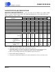
ANALOG CHARACTERISTICS (Continued)
Notes: 7. For the CS5528, the 25 mV, 55 mV and 100 mV ranges cannot be used unless NBV is powered at -1.8
to -2.5 V
8. See the section of the data sheet which discusses input models. Chop clock is 256 Hz (XIN/128) for
PGIA (programmable gain instrumentation amplifier). XIN = 32.768 kHz.
9. The maximum full scale signal can be limited by saturation of circuitry within the internal signal path.
Parameter Min Typ Max Unit
Analog Input
Common Mode + Signal on AIN+ or AIN- Bipolar/Unipolar Mode
NBV = -1.8 to -2.5 V Range = 25 mV, 55 mV, or 100 mV
Range = 1 V, 2.5 V, or 5 V
NBV = AGND Range = 25 mV, 55 mV, or 100 mV (Note 7)
Range = 1 V, 2.5 V, or 5 V
-0.150
NBV
1.85
0.0
-
-
-
-
0.950
VA+
2.65
VA+
V
V
V
V
CVF Current on AIN+ or AIN- (Note 8)
Range = 25 mV, 55 mV, or 100 mV
Range = 1 V, 2.5 V, or 5 V
-
-
100
10
300
-
pA
nA
Input Current Drift (Note 8)
Range = 25 mV, 55 mV, or 100 mV - 1 - pA/°C
Input Leakage for Multiplexer when Off - 10 - pA
Common Mode Rejection dc
50, 60 Hz
-
-
120
120
-
-
dB
dB
Input Capacitance - 10 - pF
Voltage Reference Input
Range (VREF+) - (VREF-) 1 2.5 VA+ V
VREF+
(VREF-)+1
-VA+V
VREF- NBV -
(VREF+)-1
V
CVF Current (Note 8) - 5.0 - nA
Common Mode Rejection dc
50, 60 Hz
-
-
110
130
-
-
dB
dB
Input Capacitance - 16 - pF
System Calibration Specifications
Full Scale Calibration Range (VREF = 2.5V) Bipolar/Unipolar Mode
25 mV
55 mV
100 mV
1 V
2.5 V
5 V
10
25
40
0.40
1.0
2.0
-
-
-
-
-
-
32.5
71.5
105
1.30
3.25
VA+
mV
mV
mV
V
V
V
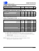
Offset Calibration Range Bipolar/Unipolar Mode
25 mV
55 mV
100 mV (Note 9)
1 V
2.5 V
5 V
-
-
-
-
-
-
-
-
-
-
-
-
±12.5
±27.5
±50
±0.5
±1.25
±2.50
mV
mV
mV
V
V
V