
User Manual


CS5521/22/23/24/28
DS317F8 5
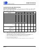
CHARACTERISTICS AND SPECIFICATIONS
ANALOG CHARACTERISTICS (T
A
= 25° C; VA+, VD+ = 5 V ±5%; VREF+ = 2.5 V, VREF- = AGND,
NBV = -2.1 V, XIN = 32.768 kHz, CFS1-CFS0 = ‘00’, OWR (Output Word Rate) = 15 Sps, Bipolar Mode, Input
Range = ±100 mV; See Notes 1 and 2.)
Notes: 1. Applies after system calibration at any temperature within -40° C ~ +85° C.
2. Specifications guaranteed by design, characterization, and/or test.
3. Specification applies to the device only and does not include any effects by external parasitic
thermocouples. LSB
N
: N is 16 for the CS5521/23 and N is 24 for the CS5522/24/28
4. Drift over specified temperature range after calibration at power-up at 25° C.
5. Measured with Charge Pump Drive off.
6. All outputs unloaded. All input CMOS levels and the CS5521/23 do not have a low power mode.
Parameter
CS5521/23 CS5522/24/28
UnitMin Typ Max Min Typ Max
Accuracy
Resolution - - 16 - - 24 Bits
Linearity Error - ±0.0015 ±0.003 - ±0.0007 ±0.0015 %FS
Bipolar Offset (Note 3) - ±1±2 -±16 ±32 LSB
N
Unipolar Offset (Note 3) - ±2 ±4-±32 ±64 LSB
N
Offset Drift (Notes 3 and 4) - 20 - - 20 - nV/°C
Bipolar Gain Error - ±8 ±31 - ±8 ±31 ppm
Unipolar Gain Error - ±16 ±62 - ±16 ±62 ppm
Gain Drift (Note 4) - 1 3 - 1 3 ppm/°C
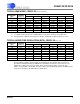
Power Supplies
Power Supply Currents (Normal Mode)
I
A+
(Note 5)I
D+
I
NBV
-
-
-
1.2
110
400
1.6
150
570
-
-
-
1.5
110
525
2.1
150
700
mA
µA
µA
Power Consumption (Note 6)
Normal Mode
Low Power Mode
Sleep
-
N/A
-
7.0
N/A
500
10
N/A
-
-
-
-
10.1
5.5
500
14.8
7.5
-
mW
mW
µW
Power Supply Rejection
Positive Supplies
dc NBV
-
-
120
110
-
-
-
-
120
110
-
-
dB
dB