
User Manual


CS5521/22/23/24/28
DS317F8 43
1.8 Power Supply Arrangements
The CS5521/22/23/24/28 A/D converters are de-
signed to operate from a single +5 V analog supply
and a single +5 V or +3 V digital supply. A -2.1 V
supply is usually generated from the charge pump
drive to provide power to the instrumentation am-
plifier’s NBV (negative bias voltage) pin.
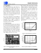
Figure 21 illustrates the CS5522 connected with a
+5 V analog supply and with the external compo-
nents required for the charge pump drive. This en-
ables the CS5522 to measure ground-referenced
signals with magnitudes down to ±100 mV.
Figure 22 illustrates the CS5522 connected to mea-
sure ground-referenced unipolar signals of a posi-
tive polarity using the 1 V, 2.5 V, and 5 V ranges
on the converter. For the 25 mV, 55 mV, and
100 mV ranges, the signals being digitized must
have a common mode between +1.85 to +2.65 V
(NBV = 0 V).
Although CS5521/22/23/24/28 are optimized for
the measurement of thermocouple outputs, they are
also well suited for the measurement of ratiometric
bridge transducer outputs. Figure 23 illustrates the
CS5522 connected to measure the output of a rati-
ometric differential bridge transducer while operat-
ing from a single +5 V supply. Bridge outputs may
range from 5 mV to 400 mV. See “Digital Gain
Scaling” on page 45 section about manipulating the
gain register to achieve optimum gain scaling.
XOUT
VD+
VA+
VREF+
VREF-
DGNDNBV
AIN1+
SCLK
SDO
SDI
CS5522
XIN
CPD
CS
10
Ω
+5V
Analog
Supply
0.1
μ
F0.1
μ
F
20
19
3
1
AGND
214
11
10
15
12
8
9
135
Optional
Clock
Source
Serial
Data
Interface
7
32.768 ~ 100 kHz
2.5V
Up to ± 100 mV Input
AIN1-
4
10 k
Ω
0.1
μ
F
10
μ
F
1N4148
1N4148
+
BAV199
18
AIN2+
17
AIN2-
16
A1
6
A0
Charge-pump network
for V D + = 5V only and
XIN = 32.768 kHz.
Logic Outputs:
A0 - A1 Switch from
VA+ to AGND.
10 k
Ω
301
Ω
499
Ω
+5V
V+
R
LM334
Absolute
Current
Reference
V-
Cold Junction
BAT85
0.033
μ
F
Figure 21. CS5522 Configured to use on-chip charge pump to supply NBV