
User Manual


CS5521/22/23/24/28
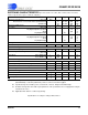
DS317F8 11
SWITCHING CHARACTERISTICS (T
A
= 25° C; VA+ = 5 V ±5%; VD+ = 3.0 V ±10% or 5 V ±5%;
Levels: Logic 0 = 0 V, Logic 1 = VD+; C
L
= 50 pF.))
Notes: 25. Device parameters are specified with a 32.768 kHz clock; however, clocks up to 200 kHz
(CS5522/24/28) or 130 kHz (CS5521/23) can be used for increased throughput.
26. Specified using 10% and 90% points on waveform of interest. Output loaded with 50 pF.
27. Oscillator start-up time varies with crystal parameters. This specification does not apply when using an
external clock source.
28. Applicable when SCLK is continuously running.
Specifications are subject to change without notice.
Parameter Symbol Min Typ Max Unit
Master Clock Frequency (Note 25)
External Clock or Internal Oscillator (CS5522/24/28)
(CS5521/23)
XIN
30
30
32.768
32.768
200
130
kHz
kHz
Master Clock Duty Cycle 40 - 60 %
Rise Times (Note 26)
Any Digital Input Except SCLK
SCLK
Any Digital Output
t
rise
-
-
-
-
-
50
1.0
100
-
µs
µs
ns
Fall Times (Note 26)
Any Digital Input Except SCLK
SCLK
Any Digital Output
t
fall
-
-
-
-
-
50
1.0
100
-
µs
µs
ns
Start-up
Oscillator Start-up Time XTAL = 32.768 kHz (Note 27) t
ost
-500-ms
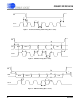
Serial Port Timing
Serial Clock Frequency SCLK 0 - 2 MHz
SCLK Falling to CS
Falling for continuous running SCLK
(Note 28)
t
0
100 - - ns
Serial Clock Pulse Width High
Pulse Width Low
t
1
t
2
250
250
-
-
-
-
ns
ns
SDI Write Timing
CS
Enable to Valid Latch Clock t
3
50 - - ns
Data Set-up Time prior to SCLK rising t
4
50 - - ns
Data Hold Time After SCLK Rising t
5
100 - - ns
SCLK Falling Prior to CS
Disable t
6
100 - - ns
SDO Read Timing
CS
to Data Valid t
7
--150ns
SCLK Falling to New Data Bit t
8
--150ns
CS
Rising to SDO Hi-Z t
9
--150ns