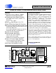
CS5521/22/23/24/28 16-bit or 24-bit, 2/4/8-channel ADCs with PGIA Features General Description Low The CS5521/22/23/24/28 are highly integrated ΔΣ analog-to-digital converters (ADCs) which use chargebalance techniques to achieve 16-bit (CS5521/23) and 24-bit (CS5522/24/28) performance. The ADCs come as either two-channel (CS5521/22), four-channel (CS5523/24), or eight-channel (CS5528) devices and include a low-input-current, chopper-stabilized instrumentation amplifier.
CS5521/22/23/24/28 TABLE OF CONTENTS ANALOG CHARACTERISTICS ................................................................................................ 5 TYPICAL RMS NOISE, CS5521/23.......................................................................................... 7 TYPICAL NOISE FREE RESOLUTION (BITS), CS5521/23 .................................................... 7 TYPICAL RMS NOISE, CS5522/24/28.....................................................................................
CS5521/22/23/24/28 2. 3. 4. 5. 6. 7. DS317F8 1.4.3 Example of Using the CSRs to Perform Conversions and Calibrations .............. 38 1.5 Conversion Output Coding .............................................................................................. 40 1.5.1 Conversion Data FIFO Descriptions ................................................................... 41 1.6 Digital Filter ....................................................................................................................
CS5521/22/23/24/28 LIST OF FIGURES Figure 1. Continuous Running SCLK Timing (Not to Scale) ......................................................... 12 Figure 2. SDI Write Timing (Not to Scale) ..................................................................................... 12 Figure 3. SDO Read Timing (Not to Scale) ................................................................................... 12 Figure 4. Multiplexer Configurations.................................................................
CS5521/22/23/24/28 CHARACTERISTICS AND SPECIFICATIONS ANALOG CHARACTERISTICS (TA = 25° C; VA+, VD+ = 5 V ±5%; VREF+ = 2.5 V, VREF- = AGND, NBV = -2.1 V, XIN = 32.768 kHz, CFS1-CFS0 = ‘00’, OWR (Output Word Rate) = 15 Sps, Bipolar Mode, Input Range = ±100 mV; See Notes 1 and 2.) CS5521/23 Parameter CS5522/24/28 Min Typ Max Min Typ Max Unit Resolution - - 16 - - 24 Bits Linearity Error - ±0.0015 ±0.003 - Accuracy ±0.0007 ±0.
CS5521/22/23/24/28 ANALOG CHARACTERISTICS (Continued) Parameter Min Typ Max Unit Common Mode + Signal on AIN+ or AINBipolar/Unipolar Mode NBV = -1.8 to -2.5 V Range = 25 mV, 55 mV, or 100 mV Range = 1 V, 2.5 V, or 5 V NBV = AGND Range = 25 mV, 55 mV, or 100 mV (Note 7) Range = 1 V, 2.5 V, or 5 V -0.150 NBV 1.85 0.0 - 0.950 VA+ 2.65 VA+ V V V V CVF Current on AIN+ or AIN(Note 8) Range = 25 mV, 55 mV, or 100 mV Range = 1 V, 2.
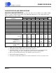
CS5521/22/23/24/28 TYPICAL RMS NOISE, CS5521/23 (Notes 10 and 11) Output Rate -3 dB Filter (Sps) Frequency 1.88 1.64 3.76 3.27 7.51 6.55 15.0 12.7 30.0 25.4 61.6 (Note 12) 50.4 84.5 (Note 12) 70.7 101.1 (Note 12) 84.6 25 mV 90 nV 122 nV 180 nV 280 nV 580 nV 2.6 µV 11 µV 41 µV Input Range, (Bipolar/Unipolar Mode) 55 mV 100 mV 1V 2.5 V 148 nV 220 nV 1.8 µV 3.9 µV 182 nV 310 nV 2.6 µV 5.7 µV 267 nV 435 nV 3.7 µV 8.5 µV 440 nV 810 nV 5.7 µV 14 µV 1.1 µV 2.1 µV 18.2 µV 48 µV 4.9 µV 8.
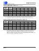
CS5521/22/23/24/28 TYPICAL RMS NOISE, CS5522/24/28 (Notes 14 and 15) Output Rate -3 dB Filter (Sps) Frequency 1.88 1.64 3.76 3.27 7.51 6.55 15.0 12.7 30.0 25.4 61.6 (Note 16) 50.4 84.5 (Note 16) 70.7 101.1 (Note 16) 84.6 25 mV 90 nV 110 nV 170 nV 250 nV 500 nV 2 µV 10 µV 30 µV Input Range, (Bipolar/Unipolar Mode) 55 mV 100 mV 1V 2.5 V 95 nV 140 nV 1.5 µV 3 µV 130 nV 190 nV 2 µV 4 µV 200 nV 275 nV 2.5 µV 6 µV 330 nV 580 nV 4.5 µV 10 µV 1 µV 1.
CS5521/22/23/24/28 5 V DIGITAL CHARACTERISTICS (TA = 25° C; VA+, VD+ = 5 V ±5%; GND = 0; See Notes 2 and 18.)) Parameter Symbol Min Typ Max Unit High-level Input Voltage All Pins Except XIN and SCLK XIN SCLK VIH 0.6 VD+ (VD+)-0.5 (VD+) - 0.45 - - V V V Low-level Input Voltage All Pins Except XIN and SCLK XIN SCLK VIL - - 0.8 1.5 0.6 V V V High-level Output Voltage All Pins Except CPD and SDO (Note 19) CPD, Iout = -4.0 mA SDO, Iout = -5.0 mA VOH (VA+) - 1.0 (VD+) - 1.0 (VD+) - 1.
CS5521/22/23/24/28 DYNAMIC CHARACTERISTICS Parameter Symbol Ratio Unit Modulator Sampling Frequency fs XIN/4 Hz Filter Settling Time to 1/2 LSB (Full-scale Step) ts 1/fout s RECOMMENDED OPERATING CONDITIONS (AGND, DGND = 0 V; See Note 20.) Parameter DC Power Supplies Positive Digital Positive Analog Analog Reference Voltage (VREF+) - (VREF-) Negative Bias Voltage Symbol Min Typ Max Unit VD+ VA+ 2.7 4.75 5.0 5.0 5.25 5.25 V V VRefdiff 1.0 2.5 VA+ V NBV -1.8 -2.1 -2.
CS5521/22/23/24/28 SWITCHING CHARACTERISTICS (TA = 25° C; VA+ = 5 V ±5%; VD+ = 3.0 V ±10% or 5 V ±5%; Levels: Logic 0 = 0 V, Logic 1 = VD+; CL = 50 pF.)) Parameter Symbol Min Typ Max Unit Master Clock Frequency (Note 25) External Clock or Internal Oscillator (CS5522/24/28) (CS5521/23) XIN 30 30 32.768 32.768 200 130 kHz kHz 40 - 60 % - 50 1.0 100 - µs µs ns - 50 1.
CS5521/22/23/24/28 CS t0 t6 t1 t3 SCLK t2 Figure 1. Continuous Running SCLK Timing (Not to Scale) CS t3 SDI M SB M S B -1 t4 LS B t5 t1 t6 S C LK t2 Figure 2. SDI Write Timing (Not to Scale) CS t9 t7 SDO M SB M S B -1 LS B t8 t2 SCLK t1 Figure 3.
CS5521/22/23/24/28 1. GENERAL DESCRIPTION The CS5521/22/23/24/28 are highly integrated ΔΣ Analog-to-Digital Converters (ADCs) which use charge-balance techniques to achieve 16-bit (CS5521/23) and 24-bit (CS5522/24/28) performance. The ADCs come as either two-channel (CS5521/22), four-channel (CS5523/24), or eightchannel (CS5528) devices, and include a low input current, chopper-stabilized instrumentation amplifier. To permit selectable input spans of 25 mV, 55 mV, 100 mV, 1 V, 2.
CS5521/22/23/24/28 1.1.1 Instrumentation Amplifier The instrumentation amplifier is chopper stabilized and is activated any time conversions are performed with the low-level input ranges, ≤100 mV. The amplifier is powered from VA+ and from the NBV (Negative Bias Voltage) pin allowing the CS5521/22/23/24/28 to be operated in either of two analog input configurations. The NBV pin can be biased to a negative voltage between -1.8 V and -2.5 V, or tied to AGND (for the CS5528, NBV has to be between -1.
CS5521/22/23/24/28 1.1.3 Analog Input Span Considerations The CS5521/22/23/24/28 is designed to measure full-scale ranges of 25 mV, 55 mV, 100 mV, 1 V, 2.5 V, and 5 V. Other full scale values can be accommodated by performing a system calibration within the limits specified. See the Calibration section for more details. Another way to change the full scale range is to increase or to decrease the voltage reference to a voltage other than 2.5 . See the Voltage Reference section for more details.
CS5521/22/23/24/28 mentation amplifier with a gain range setting of 100 mV or less, is typically 100 pA. This is low enough to permit large external resistors to divide down a large external signal without significant loading. Figure 7 illustrates an example circuit. Refer to Application Note 158 for more details on high-voltage (>5 V) measurement. 1.1.5 Voltage Reference The CS5521/22/23/24/28 devices are specified for operation with a 2.
CS5521/22/23/24/28 mentation amplifier, and providing a number of flags which indicate converter operation. A group of registers, called Channel Set-up Registers, are also included in the converters. These registers are used to hold pre-loaded conversion instructions. Each channel set-up register is 24 bits wide and holds two 12-bit conversion instructions (Setups). Upon power-up, these registers can be initialized by the user’s microcontroller with conversion instructions.
CS5521/22/23/24/28 1.2.1 System Initialization After power is first applied to the CS5521/22/2324/28 devices, the user should wait for the oscillator to start before attempting to communicate with the converter. If a 32.768 kHz crystal is used, this may be 500 milliseconds. The initialization sequence should be as follows: Initialize the serial port by sending the port initialization sequence of 15 bytes of all 1's followed by one byte with the following bit contents '1111 110'.
CS5521/22/23/24/28 1.2.2 Command Register Quick Reference D7(MSB) D6 D5 D4 D3 D2 D1 D0 CB CS2 CS1 CS0 R/W RSB2 RSB1 RSB0 BIT NAME D7 Command Bit, CB D6-D4 Channel Select Bits, CSB2-CSB0 D3 Read/Write, R/W D2-D0 Register Select Bit, RSB2-RSB0 VALUE 0 1 000 . . 111 0 1 000 001 010 011 101 FUNCTION Must be logic 0 for these commands. See table below. CS2-CS0 provide the address of one of the eight physical channels.
CS5521/22/23/24/28 1.2.3 Command Register Descriptions READ/WRITE INDIVIDUAL OFFSET CALIBRATION REGISTER D7(MSB) 0 Function: D6 CS2 D5 CS1 D4 CS0 D3 R/W D2 0 D1 0 D0 1 These commands are used to access each offset register separately. CS1 - CS0 decode the registers accessed. R/W (Read/Write) 0 Write to selected register. 1 Read from selected register.
CS5521/22/23/24/28 READ/WRITE CONFIGURATION REGISTER D7(MSB) 0 Function: D6 0 D5 0 D4 0 D3 R/W D2 0 D1 1 D0 1 These commands are used to read from or write to the configuration register. R/W (Read/Write) 0 Write to selected register. 1 Read from selected register. READ/WRITE CHANNEL-SETUP REGISTER(S) D7(MSB) 0 Function: D6 0 D5 0 D4 0 D3 R/W D2 1 D1 0 D0 1 These commands are used to access the channel-setup registers (CSRs).
CS5521/22/23/24/28 PERFORM CONVERSION D7(MSB) 1 Function: D6 CSRP3 D5 CSRP2 D4 CSRP1 D3 CSRP0 D2 0 D1 0 D0 0 These commands instruct the ADC to perform conversions on the physical input channel pointed to by the pointer bits (CSRP2 - CSRP0) in the channel-setup registers. The particular type of conversion performed is determined by the states of the conversion control bits (the multiple conversion bit, the loop bit, read convert bit, and the depth pointer bits) in the configuration register.
CS5521/22/23/24/28 PERFORM CALIBRATION D7(MSB) 1 Function: D6 CSRP3 D5 CSRP2 D4 CSRP1 D3 CSRP0 D2 CC2 D1 CC1 D0 CC0 These commands instruct the ADC to perform a calibration on the physical input channel referenced which is chosen by the command byte pointer bits (CSRP3 - CRSP0).
CS5521/22/23/24/28 SYNC1 D7(MSB) 1 Function: D6 1 D5 1 D4 1 D3 1 D2 1 D1 1 D0 1 D2 1 D1 1 D0 0 D2 0 D1 0 D0 0 Part of the serial port re-initialization sequence. SYNC0 D7(MSB) 1 Function: D6 1 D5 1 D4 1 D3 1 End of the serial port re-initialization sequence. NULL D7(MSB) 0 Function: 24 D6 0 D5 0 D4 0 D3 0 This command is used to clear a port flag and keep the converter in the continuous conversion mode.
CS5521/22/23/24/28 1.2.4 Serial Port Interface The CS5521/22/23/24/28’s serial interface consists of four control lines: CS, SCLK, SDI, SDO. Figure 10 illustrates the serial sequence necessary to write to, or read from the serial port’s registers. CS (Chip Select) is the control line which enables access to the serial port. If the CS pin is tied low, the port can function as a three-wire interface. SDI (Serial Data In) is the data signal used to transfer data to the converters.
CS5521/22/23/24/28 1.2.5 Reading/Writing the Offset, Gain, and Configuration Registers The CS5521/22/23/24/28’s offset, gain, and configuration registers are accessed individually and can be read from or written to. To write to an offset, a gain, or the configuration register, the user must transmit the appropriate write command which accesses the particular register and then follow that command with 24 bits of data (refer to Figure 10 for details).
CS5521/22/23/24/28 CSR (Channel-Setup Register) CSR #1 Setup 1 Bits <47:36> Setup 2 Bits <35:24> #2 Setup 3 Bits <23:12> Setup 4 Bits <11:0> CSR #1 Setup 1 Setup 2 Bits <95:84> Bits <83:72> #1 #4 Setup 7 Setup 8 Bits <23:12> Bits <11:0> #8 CS5521/22 Setup 1 Setup 2 Bits <191:180> Bits <179:168> Setup 15 Bits <23:12> CS5523/24 Setup 16 Bits <11:0> CS5528 D23(MSB) D22 D21 D20 D19 D18 D17 D16 D15 D14 D13 D12 A1 A0 CS2 CS1 CS0 WR2 WR1 WR0 G2 G1 G0 U/B D11 D10 D9
CS5521/22/23/24/28 1.2.6.1 Latch Outputs 1.2.7 Configuration Register The A1-A0 pins mimic the latch output, D23/D11D22/D10, bits of the channel-setup registers. A1-A0 can be used to control external multiplexers and other logic functions outside the converter. The outputs can sink or source at least 1 mA, but it is recommended to limit drive currents to less than 20 μA to reduce self-heating of the chip.
CS5521/22/23/24/28 sume 9.0 mW. The CS5521/23 typically consume 6.0 mW. The low-power mode is an alternate mode in the CS5522/24/28 that reduces the consumed power to 5.5 mW. It is entered by setting bit D8 (the low-power mode bit) in the configuration register to logic 1. Slightly degraded noise or linearity performance should be expected in the low-power mode. Note that the XIN clock should not exceed 130 kHz in low-power mode.
CS5521/22/23/24/28 D23(MSB) D22 D21 D20 D19 D18 D17 D16 D15 D14 D13 D12 NU NU CFS1 CFS0 NU MC LP RC DP3 DP2 DP1 DP0 D11 D10 D9 D8 D7 D6 D5 D4 D3 D2 D1 D0 PSS PD PS/R LPM RS RV OD OF NU NU NU NU BIT NAME VALUE FUNCTION Must always be logic 0. D23-D22 Not Used, NU 00 R D21-D20 Chop Frequency Select, CFS1-CFS0 00 01 10 11 D19 D18 Not Used, NU Multiple Conversion, MC 0 0 1 D17 Loop, LP 0 R 256 Hz Amplifier chop frequency. (XIN = 32.
CS5521/22/23/24/28 1.3 Calibration The CS5521/22/23/24/28 offer four different calibration functions including self calibration and system calibration. However, after the devices are reset, the converter is functional and can perform measurements without being calibrated. In this case, the converter will utilize the initialized values of the on-chip registers (Gain = 1.0, Offset = 0.0) to calculate output words for the ±100 mV range.
CS5521/22/23/24/28 offset to occur in the 25 mV, 55 mV, and 100 mV ranges, the AIN- pin must be at the proper common-mode voltage as specified in ‘Common Mode +Signal AIN+/-’ specification in the Analog Input section (if AIN- = 0 V, NBV must be between 1.8 V to -2.5 V). For self calibration of offset in the 1.0 V, 2.5 V, and 5 V ranges, the inputs of the modulator are connected together and then routed to the VREF- pin as shown in Figure 12.
CS5521/22/23/24/28 perform a system gain calibration. In either case, the calibration signals must be within the specified calibration limits for each specific calibration step (refer to the ‘System Calibration Specifications’ in ANALOG CHARACTERISTICS). If a system gain calibration is performed the following conditions must be met: External Connections + + AIN+ 0V +- X20 - - AIN- CM +- Figure 15.
CS5521/22/23/24/28 The variables are defined below.
CS5521/22/23/24/28 conversion words deep. Further note that the type of conversion(s) performed and the way to access the resulting data from the FIFO is determined by the MC (multiple conversion), the LP (loop), the RC (read convert), and the DP (depth pointer) bits in the configuration register. 1.4.
CS5521/22/23/24/28 SDO line. If, during the first 8 SCLKs, "00000000" is provided on SDI, the converter will remain in this conversion mode, and continue to perform conversions on the selected Setup. To exit this conversion mode, "11111111" must be provided on SDI during the first 8 SCLKs. If the user decides to exit, 24 more SCLKs are required to read the final conversion word from the data register and return to command mode. 1.4.1.
CS5521/22/23/24/28 1.4.1.5 Repeated Multiple-Setup Conversions without Wait (LP = 1 MC = 1 RC = 0) In this conversion mode, the ADC will repeatedly perform conversions, referencing multiple Setups. The CSRP bits in the command word are ignored in this mode. Instead, the Depth Pointer (DP3-DP0) bits in the Configuration Register are accessed to determine the number of Setups to reference when collecting the data.
CS5521/22/23/24/28 SCLKs for each Setup referenced are required to read the conversion words from the data FIFO. The first 8 SCLKs are used to clear the SDO flag. Every 24 bits thereafter consist of the data words of each Setup that was referenced, until all of the data has been read from the part. If, during the first 8 SCLKs, "0000 0000" is provided on SDI, the converter will remain in this conversion mode, and begin performing the next set of conversions.
CS5521/22/23/24/28 SD0. After ‘1111 1111’ is provided, 24 additional SCLKs are required to transfer the last 3 bytes of conversion data before the serial port will return to the command mode. Example 3: The configuration register has the following bits as shown: DP3-DP = ‘0101’, MC = 1, LP = 0, RC = X. The command issued is ‘1XXX X000’. These settings instruct the converter to perform a single conversion on six Setups once. The order in which the channels are converted is 6, 1, 6, 2, 6, and 3.
CS5521/22/23/24/28 of the configuration register. 4) Once the CSRs are programmed, repeated conversions on up to 16 Setups can be performed by issuing only one command byte. 5) The single conversion mode also requires only one command, but whenever another or a different single conversion is wanted, this command or a modified version of it has to be issued again. 6) The NULL command is used to keep the serial port in command mode, once it is in command mode. 1.
CS5521/22/23/24/28 1.5.
CS5521/22/23/24/28 The CS5521/22/23/24/28 have eight different linear phase digital filters which set the output word rates (OWRs) shown in Table 3. These rates assume that XIN is 32.768 kHz. Each of the filters has a magnitude response similar to that shown in Figure 18. The filters are optimized to settle to full accuracy every conversion and yield better than 80 dB rejection for both 50 and 60 Hz with output word rates at or below 15.0 Sps. The converter’s digital filters scale with XIN.
CS5521/22/23/24/28 on the converter. For the 25 mV, 55 mV, and 100 mV ranges, the signals being digitized must have a common mode between +1.85 to +2.65 V (NBV = 0 V). 1.8 Power Supply Arrangements The CS5521/22/23/24/28 A/D converters are designed to operate from a single +5 V analog supply and a single +5 V or +3 V digital supply. A -2.1 V supply is usually generated from the charge pump drive to provide power to the instrumentation amplifier’s NBV (negative bias voltage) pin.
CS5521/22/23/24/28 10 Ω +5V A n a lo g S u p p ly 0 .1 μ F 0 .1 μ F 2 VA+ 20 19 14 VD+ XOUT VREF+ VREF- X IN 11 3 2 .7 6 8 ~ 1 0 0 k H z O ptio na l C lo ck S o u rce 10 C S5522 3 0 to + 5 V In p u t + C M = 0 to V A + 4 1 18 17 16 6 A IN 1+ 9 CS A IN 115 SCLK AG ND 8 A IN 2 + SDI 12 A IN 2 SDO A1 A0 NBV CPD DGND 5 7 S e ria l D ata In te rfa ce 13 Figure 22. CS5522 Configured for ground-referenced Unipolar Signals 10 Ω + 5V A n alo g S u pp ly 0.1 μ F 0.
CS5521/22/23/24/28 1.8.1 Charge Pump Drive Circuits The CPD (Charge Pump Drive) pin of the converter can be used with external components (shown in Figure 21) to develop an appropriate negative bias voltage for the NBV pin. When CPD is used to generate the NBV, the NBV voltage is regulated with an internal regulator loop referenced to VA+. Therefore, any change on VA+ results in a proportional change on NBV. With VA+ = 5 V, NBV’s regulation is set proportional to VA+ at approximately -2.1 V.
CS5521/22/23/24/28 verter stays constant but the number of codes affected is doubled because the code size has been reduced by half. The converter input ranges are specified with a voltage reference of 2.5 V. The device can be operated with the reference tied directly to the +5 V supply. When this is done, the input span of the input ranges is doubled; the 25 mV range actually becomes a 50 mV range. The gain register can be set to 2.
CS5521/22/23/24/28 be initialized to these conditions when the instrument is used in normal operation. Once calibration is ready, input the command to start conversions in DS317F8 the mode you have selected via the configuration register bits. Monitor the SDO pin for a flag that the data is ready and read conversion data.
CS5521/22/23/24/28 1.11 PCB Layout The CS5521/22/23/24/28 should be placed entirely over an analog ground plane with both the AGND and DGND pins of the device connected to the analog plane. Place the analog-digital plane split immediately adjacent to the digital portion of the chip. If separate digital (VD+) and analog (VA+) sup- 48 plies are used, it is recommended that a diode be placed between them (the cathode of the diode should point to VA+).
CS5521/22/23/24/28 2.
CS5521/22/23/24/28 2.1 Clock Generator XIN; XOUT - Crystal In; Crystal Out. A gate inside the chip is connected to these pins and can be used with a crystal to provide the master clock for the device. Alternatively, an external (CMOS compatible) clock can be supplied into the XIN pin to provide the master clock for the device. 2.2 Control Pins and Serial Data I/O CS - Chip Select. When active low, the port will recognize SCLK. When high the SDO pin will output a high impedance state.
CS5521/22/23/24/28 NBV - Negative Bias Voltage. Input pin to supply the negative supply voltage for the 20X gain instrumentation amplifier and coarse/fine charge buffers. May be tied to AGND if AIN+ and AIN- inputs are centered around +2.5 V; or it may be tied to a negative supply voltage (-2.1 V typical) to allow the amplifier to handle low level signals more negative than ground.
CS5521/22/23/24/28 3. SPECIFICATION DEFINITIONS Linearity Error The deviation of a code from a straight line which connects the two endpoints of the A/D Converter transfer function. One endpoint is located 1/2 LSB below the first code transition and the other endpoint is located 1/2 LSB beyond the code transition to all ones. Units in percent of full-scale. Differential Nonlinearity The deviation of a code's width from the ideal width. Units in LSBs.
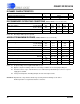
CS5521/22/23/24/28 4. ORDERING INFORMATION Model Number Bits CS5521-ASZ 16 CS5522-ASZ 24 CS5523-ASZ 16 CS5524-ASZ CS5528-ASZ 24 Channels Linearity Error (Max) 2 4 8 ±0.003% ±0.0015% Package 20-pin 0.2" Plastic SSOP (Lead Free) ±0.003% ±0.0015% Temperature Range -40°C to +85°C 24-pin 0.2" Plastic SSOP (Lead Free) 5. ENVIRONMENTAL, MANUFACTURING, & HANDLING INFORMATION Model Number CS5521-ASZ CS5522-ASZ Package Peak Reflow Temp Max Floor Life 3 260 °C 7 Days 20-pin 0.
CS5521/22/23/24/28 6. PACKAGE DIMENSION DRAWINGS 20L SSOP PACKAGE DRAWING N D E11 A2 E e b2 SIDE VIEW A ∝ A1 L END VIEW SEATING PLANE 1 2 3 TOP VIEW DIM A A1 A2 b D E E1 e L ∝ MIN -0.002 0.064 0.009 0.272 0.291 0.197 0.022 0.025 0° INCHES NOM -0.006 0.068 -0.2834 0.307 0.209 0.026 0.03 4° MAX 0.084 0.010 0.074 0.015 0.295 0.323 0.220 0.030 0.041 8° MIN -0.05 1.62 0.22 6.90 7.40 5.00 0.55 0.63 0° MILLIMETERS NOM -0.13 1.73 -7.20 7.80 5.30 0.65 0.75 4° NOTE MAX 2.13 0.25 1.88 0.38 7.
CS5521/22/23/24/28 24L SSOP PACKAGE DRAWING N D E11 A2 E e b2 SIDE VIEW A ∝ A1 L END VIEW SEATING PLANE 1 2 3 TOP VIEW DIM A A1 A2 b D E E1 e L ∝ MIN -0.002 0.064 0.009 0.311 0.291 0.197 0.022 0.025 0° INCHES NOM -0.006 0.068 -0.323 0.307 0.209 0.026 0.03 4° MAX 0.084 0.010 0.074 0.015 0.335 0.323 0.220 0.030 0.041 8° MIN -0.05 1.62 0.22 7.90 7.40 5.00 0.55 0.63 0° MILLIMETERS NOM -0.13 1.73 -8.20 7.80 5.30 0.65 0.75 4° NOTE MAX 2.13 0.25 1.88 0.38 8.50 8.20 5.60 0.75 1.
CS5521/22/23/24/28 7. REVISION HISTORY Revision Date Changes F8 JUL 2009 Leaded (Pb) and PDIP-packaged devices removed from ordering information. Contacting Cirrus Logic Support For all product questions and inquiries contact a Cirrus Logic Sales Representative. To find the one nearest to you go to www.cirrus.com IMPORTANT NOTICE Cirrus Logic, Inc. and its subsidiaries (“Cirrus”) believe that the information contained in this document is accurate and reliable.