
User guide
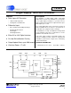


CS5509
DS125F3 9
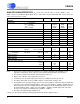
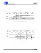
Notes: 19. All voltages with respect to ground.
20. The CS5509 can be operated with a reference voltage as low as 100 mV; but with a corresponding
reduction in noise-free resolution. The common mode voltage of the voltage reference may be any value
as long as +VREF and -VREF remain inside the supply values of VA+ and GND.
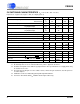
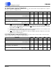
Notes: 21. No pin should go more positive than (VA+) + 0.3 V.
22. VD+ must always be less than (VA+) + 0.3 V, and can never exceed +6.0 V.
23. Applies to all pins including continuous overvoltage conditions at the analog input (AIN) pin.
24. Transient currents of up to 100 mA will not cause SCR latch-up. Maximum input current for a power
supply pin is ± 50 mA.
25. Total power dissipation, including all input currents and output currents.
*WARNING:Operation at or beyond these limits may result in permanent damage to the device.
Normal operation is not guaranteed at these extremes.
RECOMMENDED OPERATING CONDITIONS (DGND = 0V) (Note 19)
Parameter Symbol Min Typ Max Unit
DC Power Supplies Positive Digital
Positive Analog
VD+
VA+
3.15
4.75
5.0
5.0
5.5
5.5
V
V
Analog Reference Voltage (Note 20)
(VREF+) -
(VREF-) 1.0 2.5 3.6 V
Analog Input Voltage (Note 6)
Unipolar
Bipolar
VAIN
VAIN
0
-((VREF+) - (VREF-))
-
-
(VREF+) - (VREF-)
(VREF+) - (VREF-)
V
V
ABSOLUTE MAXIMUM RATINGS*
Parameter Symbol Min Typ Max Unit
DC Power Supplies Ground (Note 21)
Positive Digital (Note 22)
Positive Analog
GND
VD+
VA+
-0.3
-0.3
-0.3
-
-
-
(VD+)-0.3
6.0
6.0
V
V
V
Input Current, Any Pin Except Supplies (Notes 23 and 24)
I
in
--±10mA
Output Current
I
out
--±25mA
Power Dissipation (Total) (Note 25) - - 500 mW
Analog Input Voltage AIN and VREF pins
V
INA
-0.3 - (VA+)+0.3 V
Digital Input Voltage
V
IND
-0.3 - (VD+)+0.3 V
Ambient Operating Temperature
T
A
-40 - 85 °C
Storage Temperature
T
stg
-65 - 150 °C