
Instruction Manual
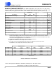
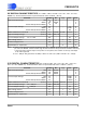
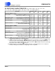

5V SWITCHING CHARACTERISTICS
(T
A
= T
MIN
to T
MAX;
VA+, VD+ = 5V
±
10%;
VA- = -5V
±
10%; Input Levels: Logic 0 = 0V, Logic 1 = VD+; C
L
= 50 pF.) (Note 2)
Parameter Symbol Min Typ Max Units
SSC Mode (M/SLP = VD+)
Access Time: CS Low to SDATA out (DRDY = low)
DRDY falling to MSB (CS = low)
t
csd1
t
dfd
-
-
-
2/f
clk
2/fclk
3/f
clk
ns
ns
SDATA Delay Time: SCLK falling to next SDATA bit t
dd1
- 80 250 ns
SCLK Delay Time SDATA MSB bit to SCLK rising t
cd1
-1/f
clk
-ns
Serial Clock (Out) Pulse Width High
Pulse Width Low
t
ph1
t
pl1
-
-
1/f
clk
1/f
clk
-
-
ns
ns
Output Float Delay: CS high to output Hi-Z (Note 16)
SCLK rising to SDATA Hi-Z
t
fd1
t
fd2
-
-
-
1/f
clk
2/f
clk
-
ns
ns
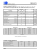
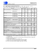
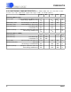
SEC Mode (M/SLP = DGND)
Serial Clock (In) f
sclk
0-2.5MHz
Serial Clock (In) Pulse Width High
Pulse Width Low
t
ph2
t
pl2
200
200
-
-
-
-
ns
ns
Access Time: CS Low to data valid (Note 17) t
csd2
- 60 200 ns
Maximum Delay time: (Note 18)
SCLK falling to new SDATA bit t
dd2
- 150 310 ns
Output Float Delay: CS high to output Hi-Z (Note 16)
SCLK falling to SDATA Hi-Z
t
fd3
t
fd4
-
-
60
160
150
300
ns
ns
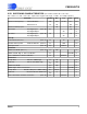
Notes: 16. If
CS is returned high before all data bits are output, the SDATA and SCLK outputs will complete the
current data bit and then go to high impedance.
17. If
CS is activated asynchronously to DRDY, CS will not be recognized if it occ urs when DRDY is high
for 2 clock cycles. The propagation delay time may be as great as 2 f
clk
cycles plus 200 ns. T o
guarantee proper clocking of SDATA when using asynchronous
CS, SCLK(i) should not be taken high
sooner than 2 f
clk
+ 200 ns after
CS goes low.
18. SDATA transitions on the falling edge of SCLK. Note that a rising SCLK must occur to enable the
serial port shifting mechanism before falling edges can be recognized.
CS5505/6/7/8
DS59F7 9
CS5505/6/7/8
DS59F7 9