
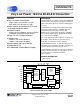
Instruction Manual
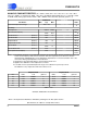
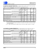

5V DIGITAL CHARACTERISTICS
(T
A
= T
MIN
to T
MAX
; VA+VD+ = 5V
±
10%; VA-= -5V
±
10%;
DGND = 0.) All measurements below are performed under static conditions. (Note 2)
Parameter Symbol Min Typ Max Units
High-Level Input Voltage: XIN
M/SLP
All Pins Except XIN and M/SLP
V
IH
V
IH
V
IH
3.5
0.9VD+
2.0
-
-
-
-
-
-
V
V
V
Low-Level Input Voltage: XIN
M/SLP
All Pins Except XIN and M/SLP
V
IL
V
IL
V
IL
-
-
-
-
-
-
1.5
0.1VD+
0.8
V
V
V
M/SLP SLEEP Active Threshold (Note 8) V
SLP
0.45VD+ 0.5VD+ 0.55VD+ V
High-Level Output Voltage (Note 9) V
OH
(VD+)-1.0 - - V
Low Level Output Vol tage I
out
= 1.6 mA V
OL
--0.4V
Input Leakage Current I
in
-110
µ
A
3-State Leakage Current I
OZ
--
±
10
µ
A
Digital Output Pi n Capacitance C
out
-9-pF
Notes: 8. Under normal operation this pin should be tied to VD+ or DGND. Anytime the voltage on the M/SLP
pin enters the SLEEP active threshold range the device will enter the power down condition. Returning
to the active state r equires elapse of the power-on reset period, the oscillator to start-up, and elapse
of the wake-up period.
9. I
out
= -100
µ
A. This guarantees the ability to drive one TTL load. (V
OH
= 2.4V @ I
out
= -40
µ
A).
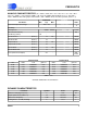
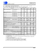
3.3V DIGITAL CHARACTERISTICS
(T
A
= T
MIN
to T
MAX
; VA+ = 5V
±
10%; VD+ = 3.3V
±
5%;
VA-= -5V
±
10%; DGND = 0.) All measurements below are performed under static conditions. (Note 2)
Parameter Symbol Min Typ Max Units
High-Level Input Voltage: XIN
M/SLP
All Pins Except XIN and M/SLP
V
IH
VIH
V
IH
0.7VD+
0.9VD+
0.6VD+
-
-
-
-
-
-
V
V
V
Low-Level Input Voltage: XIN
M/SLP
All Pins Except XIN and M/SLP
V
IL
VIL
V
IL
-
-
-
-
-
-
0.3VD+
0.1VD+
0.16VD+
V
V
V
M/SLP SLEEP Active Threshold (Note 8) V
SLP
0.43VD+ 0.45VD+ 0.47VD+ V
High-Level Output Voltage I
out
= -400 µA
V
OH
(VD+)-0.3 - - V
Low Level Output Vol tage I
out
= 400 µA
V
OL
--0.3V
Input Leakage Current I
in
-110
µA
3-State Leakage Current I
OZ
--
±10 µA
Digital Output Pi n Capacitance C
out
-9-pF
CS5505/6/7/8
DS59F7 5
CS5505/6/7/8
DS59F7 5