
Instruction Manual
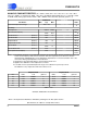
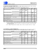
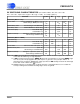
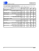

ANALOG CHARACTERISTICS
(T
A
= T
MIN
to T
MAX
; VA+ = 5V
±
10%; VA- = -5 V
±
10%; VD+ =
3.3V
±
5%; VREF+ = 2.5V (external); VREF- = 0V; f
CLK
= 32.768kHz ; Bipolar Mode; R
source
= 1k
Ω
with a
10nF to AGND at AIN; Analog input channel AIN1+; AIN- = AGND; unless otherwise specified.) (Notes 1, 2)
CS5505/7
CS5506/8 CS5507/8-S
Parameter* Min Typ Max Min Typ Max Units
Specified Temperature Range -40 to +85 -55 to +125
°
C
Analog Input
Analog Input Range: Unipolar
(VAIN+)-(VAIN-) Bi polar (Note 5)
0 to +2.5
±
2.5
0 to +2.5
±
2.5
Volts
Volts
Common Mode Rejection: dc
50, 60 Hz (Note 6)
-
120
105
-
-
-
-
120
105
-
-
-
dB
dB
Off Channel Isolation - 120 - - 120 - dB
Input Capacitance - 15 - - 15 - pF
DC Bias Current (Note 1) - 5 - - 5 - nA
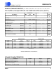
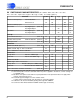
Voltage Reference (Output)
VREFOUT Voltage - (VA+)-2.5 - - (VA+)-2.5 - Volts
VREFOUT Voltage Tolerance - - 4.0 - - 4.0 %
VREFOUT Voltage Temperature Coefficient - 60 - - 60 -
ppm/
°
C
VREFOUT Line Regulation - 1.5 - - 1.5 - mV/Volt
VREFOUT Output Voltage Noise
0.1 to 10 Hz
-50- -50-
µ
V
p-p
VREFOUT: Sour ce Current
Sink Current
-
-
-
-
3
50
-
-
-
-
3
50
µ
A
µ
A
Power Supplies
DC Power Supply Currents: I
Total
I
Analog
I
Digital
-
-
-
340
300
40
450
-
-
-
-
-
340
300
40
450
-
-
µ
A
µ
A
µ
A
Power Dissipation: (Note 7)
SLEEP inactive
SLEEP active
-
-
3.2
5
4.5
10
-
-
3.2
10
4.5
25
mW
µ
W
Power Supply Rejection: Positive Supplies
Negative Supplies
-
-
80
80
-
-
-
-
80
80
-
-
dB
dB
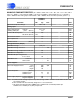
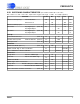
Notes: 5. Common mode voltage may be at any value as long as AIN+ and AIN- remain within the VA+ and
VA- supply voltages.
6. XIN = 32.768 kHz. Guaranteed by design and / or characterization.
7. All outputs unloaded. Al l inputs CMOS levels. SLEEP mode controlled by M/SLP pin.
SLEEP active = M/SLP pin at (VD+)/2 input level.
CS5505/6/7/8
4 DS59F7
CS5505/6/7/8
4 DS59F7