
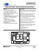
Instruction Manual
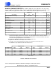
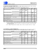
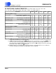

ANALOG CHARACTERISTICS
(T
A
= T
MIN
to T
MAX
; VA+ = 5V
±
10%; VA- = -5V
±
10%; VD+ =
3.3V
±
5%; VREF+ = 2.5V(external); VREF- = 0V; f
CLK
= 32.768kHz; Bipolar Mode; R
source
= 1k
Ω
with a 10nF
to AGND at AIN; Anal og input channel AIN1+; AIN- = AGND; unless otherwise specified.) (Notes 1, 2)
CS5505/7-A CS5507-S
Parameter* Min Typ Max Min Typ Max Units
Specified Temperature Range -40 to +85 -55 to +125
°
C
Accuracy
Linearity Error - 0.0015 0.003 - 0.0015 0.003
±
%FS
Differential Nonlinearity -
±
0.25
±
0.5
-
±
0.25
±
0.5
LSB
16
Full Scale Error (Note 3) -
±
0.25
±
2
-
±
0.5
±
2
LSB
16
Full Scale Drift (Note 4) -
±
0.5
--
±
2
-LSB
16
Unipolar Offset (Note 3) -
±
0.5
±
2
-
±
1
±
4
LSB
16
Unipolar Offset Drift (Note 4) -
±
0.5
--
±
1
-LSB
16
Bipolar Offset (Note 3) -
±
0.25
±
1
-
±
0.5
±
2
LSB
16
Bipolar Offset Drift (Note 4) -
±
0.25
--
±
0.5
-LSB
16
Noise (Referred to Output) - 0.16 - - 0.16 - LSB-
rms
16
Notes: 1. The AIN pin presents a very high input resistance at dc and a minor dynamic load which scales to the
master clock frequency. Both sour ce resistance and shunt capacitance are therefore critical in
determining the CS5505/6/7/8’s source impedance requirements. For more information refer to the
text section
Analog Input Impedance Consi derations.
2. Specifications guaranteed by desi gn, characterization and/or test.
3. Applies after calibration at the temperature of interest.
4. Total drift over the specified temperature range since calibration at power-up at 25
°
C.
Recalibration at any temperature will remove these errors.
Specifications are subject to change without notice.
* Refer to the Specification Definitions immediately following the Pin Description Section.
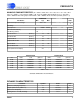
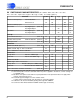
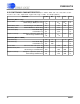
Unipolar Mode Bipolar Mode
mV LSB’s % FS ppm FS LSB’s % FS ppm FS
10 0.26 0.0004 4 0.13 0.0002 2
19 0.50 0.0008 8 0.26 0.0004 4
38 1.00 0.0015 15 0.50 0.0008 8
76 2.00 0.0030 30 1.00 0.0015 15
152 4.00 0.0061 61 2.00 0.0030 30
VREF = 2.5V
CS5505/7; 16-Bit Unit Conversion Factors
CS5505/6/7/8
2 DS59F7
CS5505/6/7/8
2 DS59F7