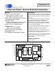
CS5505/6/7/8 CS5505/6/7/8 VeryLow Low Power, 16-bitand & 20-bit Very Power, 16-Bit 20-BitA/D A/DConverters Converters Features Description l Very The CS5505/6/7/8 are a family of low power CMOS A/D converters which are ideal for measuring low-frequency signals representing physical, chemical, and biological processes. Low Power Consumption - Single supply +5 V operation: 1.7 mW - Dual supply ±5 V operation: 3.
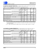
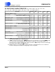
CS5505/6/7/8 CS5505/6/7/8 ANALOG CHARACTERISTICS (T A = T MIN to TMAX; VA+ = 5V ± 10%; VA- = -5 V ± 10%; VD+ = 3.3V ± 5%; VREF+ = 2.5V(external); VREF- = 0V; f CLK = 32.768kHz; Bipolar Mode; Rsource = 1kΩ with a 10nF to AGND at AIN; Anal og input channel AIN1+; AIN- = AGND; unless otherwise specified.) (Notes 1, 2) CS5505/7-A Parameter* Min Specified Temperature Range Typ CS5507-S Max Min -40 to +85 Typ Max -55 to +125 Units °C Accuracy Linearity Error - 0.0015 0.003 - 0.0015 0.
CS5505/6/7/8 CS5505/6/7/8 ANALOG CHARACTERISTICS (T A = T MIN to TMAX; VA+ = 5V ± 10%; VA- = -5 V ± 10%; VD+ = 3.3V ± 5%; VREF+ = 2.5V (external); VREF- = 0V; fCLK = 32.768kHz ; Bipolar Mode; Rsource = 1k Ω with a 10nF to AGND at AIN; Analog input channel AIN1+; AIN- = AGND; unless otherwise specified.
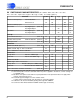
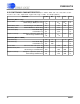
CS5505/6/7/8 CS5505/6/7/8 ANALOG CHARACTERISTICS (T A = T MIN to TMAX; VA+ = 5V ± 10%; VA- = -5 V ± 10%; VD+ = 3.3V ± 5%; VREF+ = 2.5V (external); VREF- = 0V; fCLK = 32.768kHz ; Bipolar Mode; R source = 1kΩ with a 10nF to AGND at AIN; Analog input channel AIN1+; AIN- = AGND; unless otherwise specified.) (Notes 1, 2) CS5505/7 CS5506/8 Parameter* Min Specified Temperature Range Typ CS5507/8-S Max Min Typ Max Units -40 to +85 -55 to +125 °C 0 to +2.5 ±2.5 0 to +2.5 ±2.
CS5505/6/7/8 CS5505/6/7/8 5V DIGITAL CHARACTERISTICS (T A = T MIN to TMAX; VA+VD+ = 5V ± 10%; VA-= -5V ± 10%; DGND = 0.) All measurements below are performed under static conditions. (Note 2) Parameter Symbol Min Typ Max Units High-Level Input Voltage: XIN M/SLP All Pins Except XIN and M/SLP VIH VIH VIH 3.5 0.9VD+ 2.0 - - V V V Low-Level Input Voltage: XIN M/SLP All Pins Except XIN and M/SLP VIL VIL VIL - - 1.5 0.1VD+ 0.8 V V V M/SLP SLEEP Active Threshold (Note 8) VSLP 0.45VD+ 0.
CS5505/6/7/8 CS5505/6/7/8 5V SWITCHING CHARACTERISTICS (T A = T MIN to TMAX; VA+, VD+ = 5V ± 10%; VA- = -5V ± 10%; Input Levels: Logic 0 = 0V, Logic 1 = VD+; C L = 50 pF.) (Note 2) Parameter Master Clock Frequency: Internal Oscillator: -A,B -S External Clock: Symbol Min Typ Max Units XIN or fclk 30.0 30.0 30 32.768 32.768 - 53.0 34.0 163 kHz kHz kHz 40 - 60 % Master Clock Duty Cycle Rise Times: Any Digital Input Any Digital Output (Note 10) trise - 50 1.
CS5505/6/7/8 CS5505/6/7/8 3.3V SWITCHING CHARACTERISTICS (TA = T MIN to TMAX VA+ = 5V ± 10%; VD+ = 3.3V ± 5%; VA- = -5V ± 10%; Input Levels: Logic 0 = 0V, Logic 1 = VD+ ; CL = 50 pF.) (Note 2) Parameter Master Clock Frequency: Internal Oscillator: -A,B -S External Clock: Symbol Min Typ Max Units XIN or fclk 30.0 30.0 30 32.768 32.768 - 53.0 34.0 163 kHz kHz kHz 40 - 60 % Master Clock Duty Cycle Rise Times: Any Digital Input Any Digital Output (Note 10) trise - 50 1.
CS5505/6/7/8 CS5505/6/7/8 XIN XIN/2 CAL t ccw CONV t scl STATE t cal Standby Calibration Standby Figure 1. Calibration Timing (Not to Scale) XIN XIN/2 A0, A1 t hca t sac CONV t cpw DRDY BP/UP t scn STATE Standby t con t bus Conversion t buh Standby Figure 2.
CS5505/6/7/8 CS5505/6/7/8 5V SWITCHING CHARACTERISTICS (TA = T MIN to TMAX; VA+, VD+ = 5V ± 10%; VA- = -5V ± 10%; Input Levels: Logic 0 = 0V, Logic 1 = VD+; C L = 50 pF.
CS5505/6/7/8 CS5505/6/7/8 3.3V SWITCHING CHARACTERISTICS (T A = T MIN to TMAX VA+ = 5V ± 10%; VD+ = 3.3V ± 5%; VA- = -5 V ± 10%; Input Levels: Logic 0 = 0V, Logic 1 = VD+; C L = 50 pF.
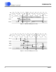
CS5505/6/7/8 CS5505/6/7/8 XIN XIN/2 CONV tcsd1 CS STATE Standby Conversion Standby Conversion DRDY tph1 SCLK(o) Hi-Z Hi-Z tdd1 tcd1 SDATA(o) Hi-Z MSB STATE (CONV held high) Conversion1 tpl1 tfd2 MSB-1 LSB+1 Hi-Z LSB Conversion2 Figure 3. Timing Relationships; SSC Mode (Not to Scale) DRDY CS SDATA(o) Hi-Z t csd2 t fd3 MSB MSB-1 MSB-2 MSB-1 LSB+2 t dd2 SCLK(i) DRDY CS SDATA(o) Hi-Z t csd2 MSB t dd2 LSB+1 LSB t fd4 t ph2 SCLK(i) t pl2 Figure 4.
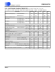
CS5505/6/7/8 CS5505/6/7/8 RECOMMENDED OPERATING CONDITIONS (DGND = 0V) (Note 19) Parameter Symbol Min Typ Max Units DC Power Supplies: Positive Digital (VA+)-(VA-) Positive Analog Negative Analog VD+ Vdiff VA+ VA- 3.15 4.75 4.5 0 5.0 10 5.0 -5.0 5.5 11 11 -5.5 V V V V 1.0 2.5 3.6 V 0 -((VREF+)-(VREF-)) - (VREF+)-(VREF-) +((VREF+)-(VREF-)) V V Analog Reference Voltage (Note 20) (VREF+)-(VREF-) Analog Input Voltage: (Note 21) Unipolar Bipolar VAIN VAIN Notes: 19.
CS5505/6/7/8 CS5505/6/7/8 GENERAL DESCRIPTION The CS5505/6/7/8 are very low power monolith ic CM OS A/D co nverters designed specifically for measurement of dc signals. The CS5505/7 are 16-bit converters (a four channel and a single channel version). The CS5506/8 are 20-bit converters (a four channel and a single channel version). Each of the devices includes a delta-sigma charge-balance converter, a voltage reference, a calibration microcontroller with SRAM, a digital filter and a serial interface.
CS5505/6/7/8 CS5505/6/7/8 slope to be used to properly scale the output digital codes when doing conversions. The calibration state is entered whenever the CAL and CONV pins are high at the same time. The state of the CAL and CONV pins at poweron and when coming out of sleep are recognized as commands, but will not be executed until the end of the 1800 clock cycle wake-up period.
CS5505/6/7/8 CS5505/6/7/8 AIN1. The BP/UP pin is not a latched input. The BP/UP pin controls how the output word from the digital filter is processed. In bipolar mode the output word computed by the digital filter is offset by 8000H in the 16-bit CS5505/7 or 80000H in 20-bit CS5506/8 (see Understanding Converter Calibration). BP/UP can be changed after a conversion is started as long as it is stable for 82 clock cycles of the conversion period prior to DRDY falling.
CS5505/6/7/8 CS5505/6/7/8 CS5505/6/7/8 +VA ages for the A/D. The differential input voltage can also have any common mode value as long as the maximum signal magnitude stays within the supply voltages. VA+ VREF+ 0.1 µF VREFVREFOUT -VA VA- Figure 6. Internal Reference Connections External reference voltages can range from 1.0 volt minimum to 3.6 volts maximum. The common mode voltage range of the external reference can allow the reference to lie at any voltage between the VA+ and VA- supply rails.
CS5505/6/7/8 CS5505/6/7/8 Understanding Converter Calibration Calibration can be performed at any time. A calibration sequence will minimize offset errors and set the gain slope scale factor. The deltasigma modulator in the converter is a differential modulator. To calibrate out offset error, the converter internally connects the modulator differential inputs to an internal VREF- voltage and measures the 1’s density output from the modulator.
CS5505/6/7/8 CS5505/6/7/8 Analog Input Impedance Considerations The analog input of the CS5505/6/7/8 can be modeled as illustrated in Figure 8 (the model ignores the multiplexer switch resistance). Capacitors (15 pF each) are used to dynamically sample each of the inputs (AIN+ and AIN-). Every half XIN cycle the switch alternately connects the capacitor to the output of the buffer and then directly to the AIN pin.
CS5505/6/7/8 CS5505/6/7/8 Digital Filter Characteristics The digital filter in the CS5505/6/7/8 is the combination of a comb filter and a low pass filter. The comb filter has zeros in its transfer function which are optimally placed to reject line interference frequencies (50 and 60 Hz and their multiples) when the CS5505/6/7/8 is clocked at 32.768 kHz. Figures 9, 10 and 11 illustrate the magnitude and phase characteristics of the filter. 0 X1 = 32.768kHz X2 = 163.
CS5505/6/7/8 CS5505/6/7/8 If the CS5505/6/7/8 is operated at a clock rate other than 32.768 kHz, the filter characteristics, including the comb filter zeros, will scale with the operating clock frequency. Therefore, optimum rejection of line frequency interference will occur with the CS5505/6/7/8 running at 32.768 kHz. The CS5505/6/7/8 can be used with external clock rates from 30 kHz to 163 kHz. ponents should be removed by means of lowpass filtering prior to the A/D input to prevent aliasing.
CS5505/6/7/8 CS5505/6/7/8 with other crystals in the range of 30 kHz to 53 kHz. Over the military temperature range (55 to +125 °C) the on-chip gate oscillator is designed to work only with a 32.768 kHz crystal. The chip will operate with external clock frequencies from 30 kHz to 163 kHz.over all temperature ranges. The 32.768 kHz crystal is normally specified as a time-keeping crystal with tight specifications for both initial frequency and for drift over temperature.
CS5505/6/7/8 CS5505/6/7/8 Synchronous External-Clocking Mode The serial port operates in the SEC mode when the M/SLP pin is connected to the DGND pin. SDATA is the output pin for the serial data. When CS goes low after new data becomes available (DRDY goes low), the SDATA pin comes out of Hi-Z with the MSB data bit present. SCLK is the input pin for the serial clock in the SEC mode. If the MSB data bit is on the SDATA pin, the first rising edge of SCLK enables the shifting mechanism.
CS5505/6/7/8 CS5505/6/7/8 analog ground pin. No analog ground pin is required because the inputs for measurement and for the voltage reference are differential and require no ground. In the digital section of the chip the supply current flows into the VD+ pin and out of the DGND pin. As a CMOS device, the CS5505/6/7/8 requires that the supply voltage on the VA+ pin always be more positive than the voltage on any other pin of the device. If this requirement is not met, the device can latch-up or be damaged.
CS5505/6/7/8 CS5505/6/7/8 Figure 14 illustrates the System Connection Diagram for the CS5505/6 using a single +5V supply. Note that all supply pins are bypassed with 0.1 µF capacitors and that the VD+ digital supply is derived from the VA+ supply. Figure 16 illustrates the CS5505/6 using dual supplies of +10V analog and +5V digital. When using separate supplies for VA+ and VD+, VA+ must be established first. VD+ should never become more positive than VA+ under any operating condition.
CS5505/6/7/8 CS5505/6/7/8 +10V Analog Supply 0.1 µF 17 (2) VA+ 20 VD+ XIN Calibration Control Bipolar/ Unipolar Input Select 4 8 CAL XOUT BP/UP M/SLP 5 6 9 10 12 13 11 *Unused analog inputs should be tied to AIN14 + Voltage (1) Reference 15 16 Signal Ground AIN1+ AIN2+ AIN3+ AIN4+ SCLK SDATA AIN- DRDY CS VREF+ A0 A1 VREF- CONV VREFOUT DGND VA- Optional Clock Source 32.768 kHz 7 CS5505/6 Analog* Signal Sources +5V Analog Supply 0.
CS5505/6/7/8 CS5505/6/7/8 PIN CONNECTIONS* CS5505/6 MULTIPLEXER SELECTION INPUT A0 1 24 A1 MULTIPLEXER SELECTION INPUT CHIP SELECT CS 2 23 DRDY DATA READY CONVERT CONV 3 22 SDATA SERIAL DATA O UTPUT CALIBRATE CAL 4 21 SCLK SERIAL CLOCK INPUT/OUTPUT CRYSTAL IN XIN 5 20 VD+ POSITIVE DIGITAL POWER CRYSTAL OUT XOUT 6 19 DGND DIGITAL GROUND RIAL MODE/ SLEEP M/SLP 7 18 VA- NEGATIVE ANALOG POWER BIPOLAR/UNIPOLAR BP/UP 8 17 VA+ POSITIVE ANALOG POWER DIFFERENTIAL ANA
CS5505/6/7/8 CS5505/6/7/8 PIN DESCRIPTIONS Pin numbers for four channel devices are in parentheses. Clock Generator XIN; XOUT - Crystal In; Crystal Out, Pins 4 (5) and 5 (6). A gate inside the chip is connected to these pins and can be used with a crystal to provide the master clock for the device. Alternatively, an external (CMOS compatible) clock can be supplied into the XIN pin to provide the master clock for the device.
CS5505/6/7/8 CS5505/6/7/8 Control Input Pins CAL - Calibrate, Pin 3 (4). When taken high the same time that the CONV pin is taken high the converter will perform a self-calibration which includes calibration of the offset and gain scale factors in the converter. CONV - Convert, Pin 2 (3). The CONV pin initiates a calibration cycle if it is taken from low to high while the CAL pin is high, or it initiates a conversion if it is taken from low to high with the CAL pin low.
CS5505/6/7/8 CS5505/6/7/8 VD+ - Positive Digital Power, Pin 17 (20). Positive digital supply voltage. Nominally +5 volts or 3.3 volts. DGND - Digital Ground, Pin 16 (19). Digital Ground. Other NC - No Connection, Pin 9. Pin should be left floating. SPECIFICATION DEFINITIONS Linearity Error The deviation of a code from a straight line which connects the two endpoints of the A/D Converter transfer function.
CS5505/6/7/8 ORDERING INFORMATION Resolution Liearity Error CS5505-ASZ (lead free) 16 Bits 0.0030% CS5506-BSZ (lead free) 20 Bits 0.0015% CS5507-ASZ (lead free) 16 Bits 0.0030% CS5508-BSZ (lead free) 20 Bits 0.
CS5505/6/7/8 REVISION HISTORY Revision Date Changes F4 MAR 1995 First Final Release F5 AUG 2005 Updated device ordering info. Updated legal notice. Added MSL data.. F7 OCT 2009 Increased minimum Vdiff voltage from 4.5 to 4.75 V. Contacting Cirrus Logic Support For all product questions and inquiries contact a Cirrus Logic Sales Representative. To find the one nearest to you go to www.cirrus.com IMPORTANT NOTICE Cirrus Logic, Inc.
CS5505/6/7/8 - NOTES - 32 DS59F7
CDB5505/6/7/8 CDB5505/6/7/8 EvaluationBoard Boardfor forCS5505/6/7/8 CS5505/6/7/8Series Seriesof ofADC’s ADCs Evaluation Description l Operation with on-board 32.768 kHz crystal The CDB5505/ 5506/5507/5508 is a ci rcuit boa rd d esigned to provide quick evaluation of the CS5505/6/7/8 series of A/D converters. The board can be configured to evaluate the CS5505/6/7/8 in either SSC (Synchronous Self-Clocking) or SEC (Synchronous External-Clocking) serial port mode.
CDB5505/6/7/8 CS5505/6/7/8 Introduction off-board reference if the connections (2A and 2B) to the bandgap IC are cut. D B Fo No rR L o ef ng er e en r A ce v a O ila nl b y le The CDB5505/6/7/8 evaluation board provides a quick means of testing the CS5505/6/7/8 series A/D converters. The CS5505/6/7/8 converters require a minimal amount of external circuitry. The evaluation board comes configured with the A/D converter chip operating from a 32.768 kHz crystal and with an off-chip precision 2.
DS59DB2 DS59DB4 -5V GND +5V AIN- AIN1+ AIN2+ AIN3+ AIN4+ + External VREF _ R12 R31 100k R30 100k R29 100k 2 100k 402 402 402 402 R7 402 4 R13 R4 R5 R6 6 0.1 µF C4 0.1 µF C5 LT1019 -2.5 V 5 10 µF R28 100k 0.1 µF +5 C9 D2 6.8V + C3 C2 D1 + 10 µF 6.8V R8 C8 25k +5 +5 1A C7 0.1 µF 16 17 R9 20 VD+ CAL 20k 3 R11 100k +5 R22 + CLKIN 3B 3A 2B 2A 1B C15 R26 1K R27 1K 0.1 µF C6 R2 200 R3 50 AIN4+ VREF- VREF+ 9 10 -5 C1 0.
CDB5505/6/7/8 CS5505/6/7/8 A0 1 CS 2/1 CONV 20/23 CS5507/8 19/22 3/2 4/3 18/21 A1 DRDY SDATA SCLK D B Fo No rR L o ef ng er e en r A ce v a O ila nl b y le CAL CS5505/6 24 XIN 5/4 17/20 VD+ XOUT 6/5 16/19 DGND M/SLP 7/6 15/18 VA- BU/UP 8/7 14/17 VA+ AIN1+ 9/8 13/16 VREFOUT 10/9 12/15 VREF- 11/10 11/14 VREF+ AIN2+/NC AIN- AIN3+ 12 13 AIN4+ Figure 2. CS5505/6 and CS5507/8 Pin Layouts for A0 and A1 (see Table 1).
CDB5505/6/7/8 C D B Fo No rR L o ef ng er e en r A ce v a O ila nl b y le CS5505/6/7/8 Figure 3.
CDB5505/6/7/8 C D B Fo No rR L o ef ng er e en r A ce v a O ila nl b y le CS5505/6/7/8 Figure 4.
CDB5505/6/7/8 C D B Fo No rR L o ef ng er e en r A ce v a O ila nl b y le CS5505/6/7/8 Figure 5.
CDB5505/6/7/8 REVISION HISTORY Revision Date DB2 MAR 1995 First Release F5 AUG 2005 Updated legal notice. JUN 2009 Removed references to part numbers for devices containing lead (Pb). D B Fo No rR L o ef ng er e en r A ce v a O ila nl b y le DB4 Changes Contacting Cirrus Logic Support For all product questions and inquiries contact a Cirrus Logic Sales Representative. To find the one nearest to you go to www.cirrus.com IMPORTANT NOTICE C Cirrus Logic, Inc.