
Manual
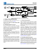
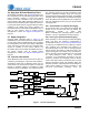

CS5490
14 DS982F3
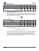
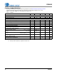
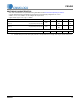
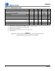
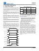
ABSOLUTE MAXIMUM RATINGS
Notes: 15. VDDA and GNDA must satisfy [(VDDA) – (GNDA)] + 4.0V.
16. Applies to all pins, including continuous overvoltage conditions at the analog input pins.
17. Transient current of up to 100mA will not cause SCR latch-up.
18. Applies to all pins, except VREF±
.
19. Total power dissipation, including all input currents and output currents.
20. Applies to all pins.
WARNING:
Operation at or beyond these limits may result in permanent damage to the device.
Normal operation is not guaranteed at these extremes.
Parameter Symbol Min Typ Max Unit
DC Power Supplies
(Note 15) VDDA -0.3 - +4.0 V
Input Current
(Notes 16 and 17)
I
IN
-- ±10mA
Input Current for Power Supplies - - - ±50 -
Output Current
(Note 18)
I
OUT
-- 100mA
Power Dissipation
(Note 19)
P
D
-- 500mW
Input Voltage
(Note 20)
V
IN
- 0.3 - (VDDA) + 0.3 V
Junction-to-Ambient Thermal Impedance
2 Layer Board
4 Layer Board
JA
-
-
140
70
-
-
°C/W
°C/W
Ambient Operating Temperature
T
A
-40 - 85 °C
Storage Temperature
T
stg
-65 - 150 °C