CS5490 Two Channel Energy Measurement IC Features Description • The CS5490 is a high-accuracy, two-channel, energy measurement analog front end. • • • • • Superior Analog Performance with Ultra-low Noise Level & High SNR Energy Measurement Accuracy of 0.
CS5490 TABLE OF CONTENTS 1. Overview . . . . . . . . . . . . . . . . . . . . . . . . . . . . . . . . . . . . . . . . . . . . . . . . . . . . . . . . . . . . . . . .5 2. Pin Description . . . . . . . . . . . . . . . . . . . . . . . . . . . . . . . . . . . . . . . . . . . . . . . . . . . . . . . . .6 2.1 Analog Pins . . . . . . . . . . . . . . . . . . . . . . . . . . . . . . . . . . . . . . . . . . . . . . . . . . . . . . . .6 2.1.1 Voltage Input . . . . . . . . . . . . . . . . . . . . . . . . . . . . . . . .
CS5490 5.9 Anti-creep . . . . . . . . . . . . . . . . . . . . . . . . . . . . . . . . . . . . . . . . . . . . . . . . . . . . . . . . 23 5.10 Register Protection . . . . . . . . . . . . . . . . . . . . . . . . . . . . . . . . . . . . . . . . . . . . . . . . 23 5.10.1 Write Protection . . . . . . . . . . . . . . . . . . . . . . . . . . . . . . . . . . . . . . . . . . . . . 23 5.10.2 Register Checksum . . . . . . . . . . . . . . . . . . . . . . . . . . . . . . . . . . . . . . . . . . 23 6.
CS5490 LIST OF FIGURES Figure 1. Oscillator Connections................................................................................................... 7 Figure 2. UART Serial Frame Format ........................................................................................... 7 Figure 3. Active Energy Load Performance.................................................................................. 8 Figure 4. Reactive Energy Load Performance...........................................................
CS5490 1. OVERVIEW The CS5490 is a CMOS power measurement integrated circuit that uses two analog-to-digital converters to measure line voltage and current. The CS5490 calculates active, reactive, and apparent power as well as RMS voltage and current and peak voltage and current. It handles other system-related functions, such as energy pulse generation, voltage sag and swell, overcurrent and zero-crossing detection, and line frequency measurement.
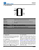
CS5490 2. PIN DESCRIPTION XOUT XIN RESET IINIIN+ VIN+ VINVREF- 1 2 3 4 5 6 7 8 16 15 14 13 12 11 10 9 VDDD MODE RX TX DO VDDA GNDA VREF+ Clock Generator Crystal In Crystal Out 2,1 XIN, XOUT — Connect to an external quartz crystal. Alternatively, an external clock can be supplied to the XIN pin to provide the system clock for the device.
CS5490 2.1.3 Voltage Reference 2.2.2 Digital Output The CS5490 generates a stable voltage reference of 2.4V between the VREF pins. The reference system also requires a filter capacitor of at least 0.1µF between the VREF pins. The CS5490 provides a configurable digital output (DO). It can be configured to output energy pulses, interrupt, zero-crossings, or energy directions. Refer to the description of the Config1 register in section 6.6 Register Descriptions on page 32 for more details.
CS5490 3. CHARACTERISTICS & SPECIFICATIONS RECOMMENDED OPERATING CONDITIONS Parameter Positive Analog Power Supply Specified Temperature Range Symbol VDDA TA Min 3.0 -40 Typ 3.3 - Max 3.6 +85 Unit V °C POWER MEASUREMENT CHARACTERISTICS Parameter Active Energy (Note 1 & 2) Reactive Energy (Note 1 & 2) Apparent Power (Note 1 & 3) Current RMS (Note 1, 3, & 4) Symbol Min Typ Max Unit All Gain Ranges Current Channel Input Signal Dynamic Range 4000:1 PAvg - ±0.
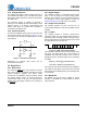
CS5490 1 Percent Error (%) 0.5 0 Lagging sin(੮) = 0.5 Leading sin(੮) = 0.5 sin(੮) = 1 -0.5 -1 0 500 1000 1500 2000 2500 3000 3500 4000 4500 Current Dynamic Range (x : 1) Figure 4. Reactive Energy Load Performance 1 Percent Error (%) 0.5 0 IRMS Error IRMS Error -0.5 -1 0 500 1000 1500 Current Dynamic range (x : 1) Figure 5.
CS5490 ANALOG CHARACTERISTICS • • • • Min/Max characteristics and specifications are guaranteed over all Recommended Operating Conditions. Typical characteristics and specifications are measured at nominal supply voltages and TA = 25°C. VDDA = +3.3V ±10%; GNDA = 0V. All voltages with respect to 0V. MCLK = 4.096MHz. Parameter Symbol Min Typ Max Unit CMRR 80 - - dB -0.
CS5490 Parameter Symbol Min Typ Max Unit PSCA - 3.9 - mA PC - 12.9 4.5 - mW mW Power Supplies Power Supply Currents (Active State) IA+ (VDDA = +3.3V) Power Consumption (Note 5) Notes: Active State (VDDA = +3.3V) Stand-by State 5. 6. 7. All outputs unloaded. All inputs CMOS level. Temperature accuracy measured after calibration is performed. Measurement method for PSRR: VDDA = +3.3V, a 150mV (zero-to-peak) (60Hz) sinewave is imposed onto the +3.3V DC supply voltage at the VDDA pin.
CS5490 DIGITAL CHARACTERISTICS • • • • Min / Max characteristics and specifications are guaranteed over all Recommended Operating Conditions. Typical characteristics and specifications are measured at nominal supply voltages and TA = 25°C. VDDA = +3.3V ±10%; GNDA = 0V. All voltages with respect to 0V. MCLK = 4.096MHz.
CS5490 SWITCHING CHARACTERISTICS • • • • Min / Max characteristics and specifications are guaranteed over all Recommended Operating Conditions. Typical characteristics and specifications are measured at nominal supply voltages and TA = 25°C. VDDA = +3.3V ±10%; GNDA = 0V. All voltages with respect to 0V. Logic Levels: Logic 0 = 0V, Logic 1 = VDDA. Parameter Rise Times (Note 13) Fall Times (Note 13) Symbol Min Typ Max Unit DO Any Digital Output Except DO trise - 50 1.
CS5490 ABSOLUTE MAXIMUM RATINGS Parameter DC Power Supplies Input Current (Note 15) (Notes 16 and 17) Input Current for Power Supplies Symbol Min Typ Max Unit VDDA -0.3 - +4.0 V IIN - - ±10 mA - - - ±50 - Output Current (Note 18) IOUT - - 100 mA Power Dissipation (Note 19) PD - - 500 mW Input Voltage (Note 20) VIN - 0.3 - (VDDA) + 0.
VIN± PMF 4th Order ΔΣ Modulator x10 MUX CS5490 DELAY CTRL IIR SINC3 V HPF Phase Shift PC ... CPCC[1:0] ... FPCC[8:0] ... SYS GAIN Config 2 I DCOFF IIN± 4th Order ΔΣ Modulator PGA DELAY CTRL SINC3 VGAIN IIR Epsilon ... VFLT[1:0] IFLT[1:0] ... 2 P I GAIN HPF INT PMF MUX VDCOFF Q I Registers Figure 6. Signal Flow for V, I, P, and Q Measurements 4. SIGNAL FLOW DESCRIPTION The signal flow for voltage, current measurement, and the other calculations is shown in Figure 6.
CS5490 4.6 High-pass & Phase Matching Filters Optional high-pass filters (HPF in Figure 6) remove any DC component from the selected signal paths. Each power calculation contains a current and voltage channel. If an HPF is enabled in only one channel, a phase-matching filter (PMF) should be applied to the other channel to match the phase response of the HPF. For AC power measurement, high-pass filters should be enabled on the voltage and current channels.
CS5490 SampleCount register should not be changed from its default value of 4000, and bit AFC of the Config2 register must be set. During continuous conversion, the host processor should not change the SampleCount register. 4.8.3 RMS Current & Voltage The root mean square (RMS in Figure 7) calculations are performed on N instantaneous voltage and current samples using Equation 1: The APCM bit in the Config2 register controls which method is used for apparent power calculation. 4.8.
CS5490 5. FUNCTIONAL DESCRIPTION 5.1 Power-on Reset (POR) Table 1. POR Thresholds The CS5490 has an internal power supply supervisor circuit that monitors the VDDA and VDDD power supplies and provides the master reset to the chip. If any of these voltages are in the reset range, the master reset is triggered. Both the analog and the digital supply have their own POR circuit. During power-up, both supplies have to be above the rising threshold for the master reset to be de-asserted.
CS5490 V(t), I(t) If |VPEAK| > VZXLEVEL, then voltage zero-crossing detection is enabled. If |IPEAK| > IZXLEVEL, then current zero-crossing detection is enabled. If |VPEAK| VZXLEVEL, then voltage zero-crossing detection is disabled. If |IPEAK| IZXLEVEL, then current zero-crossing detection is disabled. VZXLEVEL IZXLEVEL t DO Zero-crossing output on DOx pin Pulse width = 250μs t Figure 9. Zero-crossing Level and Zero-crossing Output on DO 5.
CS5490 EPG_ON (Config1) MCLK 0000 P AVG 0010 0011 Q AVG Reserved 0100 Q SUM 0101 S 0110 Reserved S SUM 0111 Energy Pulse Generation (EPG) P SUM 0001 1000 PULSE RATE (PulseCtrl) EPGIN[3:0] 4 (PulseWidth) FREQ_RNG[3:0] 4 (PulseWidth) PW[7:0] 8 Reserved 0001 Reserved 0010 Reserved 0011 P Sign 0100 Reserved 0101 PSUM Sign 0110 Q Sign 0111 Reserved 1000 Q SUM Sign 1001 Reserved 1010 V Crossing 1011 I Crossing 1100 Reserved 1101 Hi-Z 1110 Interrupt 1111 DOMODE
CS5490 The CS5490 pulse generation block behaves as follows: • The pulse rate generated by full-scale (1.0 decimal) power register is FOUT = (PulseRate x 2000)/2FREQ_RNG • The PulseRate register value is PulseRate = (FOUT x 2FREQ_RNG)/2000 = (18.5186 x 64)/2000 = 0.5925952 = 0x4BDA29 5.5.2 Pulse Width The PulseWidth register defines the Active-low time of each energy pulse: these to zero (default) disables the detect feature for the given channel. The value is in output word rate (OWR) samples.
CS5490 5.7 Phase Sequence Detection Polyphase meters using multiple CS5490 devices may be configured to sense the succession of voltage zero-crossings and determine which phase order is in service. The phase sequence detection within CS5490 involves counting the number of OWR samples from a starting point to the next voltage zero-crossing rising edge or falling for each phase.
CS5490 Write 0x16 to PSDC Register Start on the Falling Edge on the RX Pin Phase A Channel Stop 2 Phase A Count 0 -2 C Phase B Channel Stop 2 Phase B Count 0 -2 A B Phase C Channel Stop 2 Phase C Count 0 -2 Figure 13. Phase Sequence C, B, A for Rising Edge Transition be write-protected from the calculation engine. Setting 5.8 Temperature Measurement the DSP_LCK[4:0] bits to 0x09 disables the The CS5490 has an internal temperature sensor, which write-protection mode.
CS5490 6. HOST COMMANDS AND REGISTERS 6.1 Host Commands 6.1.1.3 Register Write The first byte sent to the CS5490 RX pin contains the host command. Four types of host commands are required to read and write registers and instruct the calculation engine. The two most significant bits (MSBs) of the host command defines the function to be performed. The following table depicts the types of commands. A register write command is designated by setting the two MSBs of the command to binary ‘01’.
CS5490 6.1.3 Checksum To improve the communication reliability on the serial interface, the CS5490 provides a checksum mechanism on transmitted and received signals. Checksum is disabled by default but can be enabled by setting the appropriate bit in the SerialCtrl register. When enabled, both host and CS5490 are expected to send one additional checksum byte after the normal command byte and applicable 3-byte register data have been transmitted.
CS5490 6.
CS5490 53 54 55 56 57 58 59 60 61 62 63 Notes: 11 0101 11 0110 11 0111 11 1000 11 1001 11 1010 11 1011 11 1100 11 1101 11 1110 11 1111 ZXNUM - Reserved Reserved Num. Zero Crosses used for Line Freq. Reserved Reserved Reserved Reserved Reserved Reserved Reserved Reserved Y - Y 0x00 0064 - (1) Warning: Do not write to unpublished or reserved register locations. (2) * Registers with checksum protection. (3) Registers that can be set to write protect from DSP and/or HOST.
CS5490 6.
CS5490 53 54* 55* 56* 57 58* 59* 60* 61 62 63 Notes: 11 0101 11 0110 11 0111 11 1000 11 1001 11 1010 11 1011 11 1100 11 1101 11 1110 11 1111 TGAIN TOFF TSETTLE LoadMIN SYSGAIN Time - Reserved Temperature Gain Temperature Offset Reserved Filter Settling Time to Conv.
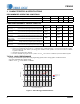
CS5490 6.4 Software Registers Summary (Page 17) Address2 0* 1* 2 3 4* 5* 6 7 8* 9* 10 11 12* 13* 14 15 16 17 18 19 20 21 22 23 24 25 26 27 28 29 30 31 RA[5:0] 00 0000 00 0001 00 0010 00 0011 00 0100 00 0101 00 0110 00 0111 00 1000 00 1001 00 1010 00 1011 00 1100 00 1101 00 1110 00 1111 01 0000 01 0001 01 0010 01 0011 01 0100 01 0101 01 0110 01 0111 01 1000 01 1001 01 1010 01 1011 01 1100 01 1101 01 1110 01 1111 Notes: (1) Warning: Do not write to unpublished or reserved register locations.
CS5490 6.
CS5490 6.6 Register Descriptions 21. “Default” = bit states after power-on or reset 22. DO NOT write a “1” to any unpublished register bit or to a bit published as “0”. 23. DO NOT write a “0” to any bit published as “1”. 24. DO NOT write to any unpublished register address. 6.6.
CS5490 6.6.2 Configuration 1 (Config1) – Page 0, Address 1 23 0 22 0 21 0 20 EPG_ON 19 0 18 0 17 0 16 DO_OD 15 1 14 1 13 1 12 0 11 1 10 1 9 1 8 0 7 1 6 1 5 1 4 0 3 DOMODE[3] 2 DOMODE[2] 1 DOMODE[1] 0 DOMODE[0] Default = 0x00 EEEE [23:21] Reserved. EPG_ON Enable EPG block. 0 = Disable energy pulse generation block (Default) 1 = Enable energy pulse generation block [19:17] Reserved. DO_OD Allow the DO pin to be an open-drain output.
CS5490 6.6.3 Configuration 2 (Config2) – Page 16, Address 0 23 - 22 POS 21 - 20 1 19 - 18 0 17 0 16 - 15 - 14 APCM 13 - 12 ZX_LPF 11 AVG_MODE 10 REG_CSUM_OFF 9 AFC 8 0 7 0 6 0 5 0 4 IFLT[1] 3 IFLT[0] 2 VFLT[1] 1 VFLT[0] 0 IIR_OFF Default = 0x10 0200 [23] Reserved. POS Positive energy only. Suppress negative values in PAVG . If a negative value is calculated, a zero result will be stored. 0 = Positive and negative energy (Default) 1 = Positive energy only [21:15] Reserved.
CS5490 6.6.4 Phase Compensation (PC) – Page 0, Address 5 23 - 22 - 21 CPCC[1] 20 CPCC[0] 19 - 18 - 17 - 16 - 15 - 14 - 13 - 12 - 11 - 10 - 9 - 8 FPCC[8] 7 6 5 4 3 2 1 0 FPCC[7] FPCC[6] FPCC[5] FPCC[4] FPCC[3] FPCC[2] FPCC[1] FPCC[0] Default = 0x00 0000 [23:22] Reserved. CPCC[1:0] Coarse phase compensation control for I & V. 00 = No extra delay 01 = 1 OWR delay in current channel 10 = 1 OWR delay in voltage channel 11 = 2 OWR delay in voltage channel [19:9] Reserved.
CS5490 6.6.6 Pulse Output Width (PulseWidth) – Page 0, Address 8 23 - 22 - 21 - 20 - 19 18 17 16 FREQ_RNG[3] FREQ_RNG[2] FREQ_RNG[1] FREQ_RNG[0] 15 PW[15] 14 PW[14] 13 PW[13] 12 PW[12] 11 PW[11] 10 PW[10] 9 PW[9] 8 PW[8] 7 6 5 4 3 2 1 0 PW[7] PW[6] PW[5] PW[4] PW[3] PW[2] PW[1] PW[0] Default = 0x00 0001 (265.6µs at OWR = 4kHz) PulseWidth sets the energy pulse frequency range and the duration of energy pulses.
CS5490 6.6.8 Pulse Output Control (PulseCtrl) – Page 0, Address 9 23 - 22 - 21 - 20 - 19 - 18 - 17 - 16 - 15 0 14 0 13 0 12 0 11 0 10 0 9 0 8 0 7 6 5 4 3 2 1 0 0 0 0 0 EPGIN[3] EPGIN[2] EPGIN[1] EPGIN[0] Default = 0x00 0000 This register controls the input to the energy pulse generation (EPG) block. [23:4] Reserved. EPGIN[3:0] Selects the input to the energy pulse generation (EPG) block.
CS5490 6.6.10 Phase Sequence Detection and Control (PSDC) – Page 0, Address 48 23 DONE 22 PSCNT[6] 21 PSCNT[5] 20 PSCNT[4] 19 PSCNT[3] 18 PSCNT[2] 17 PSCNT[1] 16 PSCNT[0] 15 - 14 - 13 - 12 - 11 - 10 - 9 - 8 - 7 - 6 - 5 DIR 4 CODE[4] 3 CODE[3] 2 CODE[2] 1 CODE[1] 0 CODE[0] Default = 0x00 0000 DONE Indicates valid count values reside in PSCNT[6:0]. 0 = Invalid values in PSCNT[6:0]. (Default) 1 = Valid values in PSCNT[6:0].
CS5490 6.6.12 Interrupt Status (Status0) – Page 0, Address 23 23 DRDY 22 CRDY 21 WOF 20 - 19 - 18 MIPS 17 - 16 VSWELL 15 - 14 POR 13 - 12 IOR 11 - 10 VOR 9 - 8 IOC 7 - 6 VSAG 5 TUP 4 FUP 3 IC 2 RX_CSUM_ERR 1 - 0 RX_TO Default = 0x 00 0000 The Status0 register indicates a variety of conditions within the chip. Writing a one to a Status0 register bit will clear that bit. Writing a zero to any bit has no effect. DRDY Data Ready.
CS5490 6.6.13 Interrupt Mask (Mask) – Page 0, Address 3 23 DRDY 22 CRDY 21 WOF 20 - 19 - 18 MIPS 17 0 16 VSWELL 15 0 14 POR 13 0 12 IOR 11 0 10 VOR 9 0 8 IOC 7 0 6 VSAG 5 TUP 4 FUP 3 IC 2 RX_CSUM_ERR 1 - 0 RX_TO Default = 0x00 0000 The Mask register is used to control the activation of the INT pin. Writing a '1' to a Mask register bit will allow the corresponding Status0 register bit to activate the INT pin when set. [23:0] Enable/disable (mask) interrupts.
CS5490 6.6.15 Chip Status 2 (Status2) – Page 0, Address 25 23 - 22 - 21 - 20 - 19 - 18 - 17 - 16 - 15 - 14 - 13 - 12 - 11 - 10 - 9 - 8 - 7 - 6 - 5 QSUM_SIGN 4 - 3 Q_SIGN 2 PSUM_SIGN 1 - 0 P_SIGN Default = 0x00 0000 This register indicates a variety of conditions within the chip. [23:6] Reserved. QSUM_SIGN Indicates the sign of the value contained in QSUM. 0 = positive value 1 = negative value [4] Reserved. Q_SIGN Indicates the sign of the value contained in QAVG.
CS5490 6.6.17 No Load Threshold (LoadMIN) – Page 16, Address 58 MSB -(20) LSB 2-1 2-2 2-3 2-4 2-5 2-6 2-7 ..... 2-17 2-18 2-19 2-20 2-21 2-22 2-23 Default = 0x00 0000 LoadMIN is used to set the no-load threshold for the anti-creep function. When the magnitudes of PSUM and QSUM are less than LoadMIN, PSUM and QSUM are forced to zero. When the magnitude of SSUM is less than LoadMIN, SSUM is forced to zero. LoadMIN is a two’s complement value in the range of -1.0 value 1.
CS5490 6.6.21 System Gain (SysGAIN ) – Page 16, Address 60 MSB LSB -(21) 20 2-1 2-2 2-3 2-4 2-5 2-6 ..... 2-16 2-17 2-18 2-19 2-20 2-21 2-22 Default = 0x50 0000 (1.25) System Gain (SysGAIN ) is applied to all channels. By default, SysGAIN = 1.25, but can be finely adjusted to compensate for voltage reference error. It is a two's complement value in the range of -2.0 value 2.0, with the binary point to the right of the second MSB. Values should be kept within 5% of 1.25. 6.6.
CS5490 6.6.25 Voltage Sag Level (VSagLEVEL ) – Page 17, Address 1 MSB -(20) LSB 2-1 2-2 2-3 2-4 2-5 2-6 2-7 ..... 2-17 2-18 2-19 2-20 2-21 2-22 2-23 Default = 0x00 0000 Voltage sag level, VSagLEVEL, establishes an input level below which a sag event is triggered. This is a two's complement value in the range of -1.0 value 1.0, with the binary point to the right of the MSB. Negative values are not used. 6.6.
CS5490 6.6.29 Voltage Swell Level (VSwellLEVEL ) – Page 18, Address 47 MSB -(20) LSB 2-1 2-2 2-3 2-4 2-5 2-6 2-7 ..... 2-17 2-18 2-19 2-20 2-21 2-22 2-23 Default = 0x7F FFFF Voltage swell level, VSwellLEVEL, establishes an input level above which a swell event is triggered. This is a two's complement value in the range of -1.0 value 1.0, with the binary point to the right of the MSB. Negative values are not used. 6.6.
CS5490 6.6.33 Active Power (PAVG) – Page 16, Address 5 MSB -(20) LSB 2-1 2-2 2-3 2-4 2-5 2-6 2-7 ..... 2-17 2-18 2-19 2-20 2-21 2-22 2-23 Default = 0x00 0000 Instantaneous power is averaged over each low-rate interval (SampleCount samples) and then added with power offset (POFF) to compute active power (PAVG). This is a two's complement value in the range of -1.0 value 1.0, with the binary point to the right of the MSB. 6.6.
CS5490 6.6.37 Instantaneous Quadrature Power (Q) – Page 16, Address 15 MSB -(20) LSB 2-1 2-2 2-3 2-4 2-5 2-6 2-7 ..... 2-17 2-18 2-19 2-20 2-21 2-22 2-23 Default = 0x00 0000 Instantaneous quadrature power, Q, the product of V shifted 90° and I. This is a two's complement value in the range of -1.0 value 1.0, with the binary point to the right of the MSB. 6.6.38 Peak Current (IPEAK) – Page 0, Address 37 MSB -(20) LSB 2-1 2-2 2-3 2-4 2-5 2-6 2-7 .....
CS5490 6.6.41 Power Factor (PF) – Page 16, Address 21 MSB -(20) LSB 2-1 2-2 2-3 2-4 2-5 2-6 2-7 ..... 2-17 2-18 2-19 2-20 2-21 2-22 2-23 Default = 0x00 0000 Power factor (PF) is calculated by dividing active power (PAVG) by apparent power (S). The sign is determined by the active power (PAVG) sign. This is a two's complement value in the range of -1.0 value 1.0, with the binary point to the right of the MSB. 6.6.
CS5490 6.6.45 Total Reactive Power (QSUM ) – Page 16, Address 31 MSB -(20) LSB 2-1 2-2 2-3 2-4 2-5 2-6 2-7 ..... 2-17 2-18 2-19 2-20 2-21 2-22 2-23 Default = 0 QSUM = QAVG This is a two's complement value in the range of -1.0 value 1.0, with the binary point to the right of the MSB. 6.6.46 DC Offset for Current (IDCOFF ) – Page 16, Address 32 MSB -(20) LSB 2-1 2-2 2-3 2-4 2-5 2-6 2-7 .....
CS5490 6.6.49 Gain for Voltage (VGAIN ) – Page 16, Address 35 MSB 21 LSB 20 2-1 2-2 2-3 2-4 2-5 2-6 ..... 2-16 2-17 2-18 2-19 2-20 2-21 2-22 Default = 1.0 Gain register VGAIN is initialized to 1.0 on reset. During gain calibration, the VGAIN register is written with the multiplicative inverse of the gain measured. This is an unsigned fixed-point value in the range of 0 value 4.0, with the binary point to the right of the second MSB. 6.6.
CS5490 6.6.54 Temperature Offset (TOFF ) – Page 16, Address 55 MSB LSB -(27) 26 25 24 23 22 21 20 ..... 2-10 2-11 2-12 2-13 2-14 2-15 2-16 Default = 0xD5 3998 Register TOFF is used to offset the Temperature register (T), and is a two's complement value in the range of -128.0value128.0 (°C), with the binary point to the right of bit 16. Register T can be rescaled by the application using the TGAIN and TOFF registers. Refer to section 7.
CS5490 7. SYSTEM CALIBRATION samples that are averaged during a calibration. The calibration procedure takes the time of N + TSETTLE OWR samples. As N is increased, the calibration takes more time, but the accuracy of the calibration results tends to increase. Component tolerances, residual ADC offset, and system noise require a meter that needs to be calibrated before it meets a specific accuracy requirement.
CS5490 result in the AC offset register. This AC offset will be subtracted from RMS measurements in subsequent conversions, removing the AC offset on the current channel. The AC offset register for the channel being calibrated should first be cleared prior to performing the calibration. The high-pass filter should be enabled if AC offset calibration is used. It is recommended that TSETTLE be set to 2000ms before performing an AC offset calibration.
CS5490 Once the phase offset is known, the CPCC and FPCC bits for that channel are calculated and programmed in the PC register. CPCC bits are used if either • The phase offset is more than 1 output word rate (OWR) sample. • More delay is needed on the voltage channel. The compensation resolution is 0.008789° at 50Hz and 0.010547° at 60Hz at an OWR of 4000Hz. 7.
CS5490 8. BASIC APPLICATION CIRCUITS The CS5490 is configured to measure power in a single-phase, two-wire single voltage and current system, as illustrated in Figure 21. In this diagram, a current transformer (CT) is used to sense the line load current, and a resistive voltage divider is used to sense the line voltage. +3.3V +3.3V 0.1µF N 0.1µF VDDA MODE VDDD Line Wh +3.3V 1K 1K 5 x250K DO VIN27nF 27nF VIN+ CS5490 RX TX ½ R BURDEN 1K CT IIN+ 4.
CS5490 9. PACKAGE DIMENSIONS 16 SOIC (150 MIL BODY) PACKAGE DRAWING Dimension A A1 b c D E E1 e L Θ aaa bbb ddd MIN -0.10 0.31 0.10 0.40 0° mm NOM ----9.90 BSC 6.00 BSC 3.90 BSC 1.27 BSC --0.10 0.25 0.25 MAX 1.75 0.25 0.51 0.25 MIN -0.004 0.012 0.004 1.27 8° 0.016 0° inch NOM ----0.390 BSC 0.236 BSC 0.154 BSC 0.05 BSC --0.004 0.010 0.010 MAX 0.069 0.010 0.020 0.010 0.050 8° Notes: 1. 2. 3. 4. 56 Controlling dimensions are in millimeters. Dimensions and tolerances per ASME Y14.5M.
CS5490 10. ORDERING INFORMATION Ordering Number Container CS5490-ISZ Bulk CS5490-ISZR Tape & Reel Temperature Package -40 to +85 °C 16-pin SOIC, Lead (Pb) Free 11. ENVIRONMENTAL, MANUFACTURING, & HANDLING INFORMATION Part Number Peak Reflow Temp MSL Rating* Max Floor Life CS5490-ISZ 260 °C 3 7 Days * MSL (Moisture Sensitivity Level) as specified by IPC/JEDEC J-STD-020. 12. REVISION HISTORY Revision Date Changes PP1 APR 2012 Preliminary release.