
User guide

CS5480
6 DS980F3
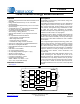
2. PIN DESCRIPTION
Clock Generator
Crystal In
Crystal Out
1,24
XIN, XOUT — Connect to an external quartz crystal. Alternatively, an external clock can be
supplied to the XIN pin to provide the system clock for the device.
Digital Pins and Serial Data I/O
Digital Outputs 13,14,15
DO1, DO2, DO3 — Configurable digital outputs for energy pulses, interrupt, tamper indication,
energy direction, and zero-crossings.
Reset 2
RESET — An active-low Schmitt-trigger input used to reset the chip.
Serial Data I/O 16,17
TX/SDO, RX/SDI — UART/SPI serial data output/input.
Serial Clock Input 18
SCLK — Serial clock for the SPI.
Serial Mode Select 20
SSEL — Selects the type of the serial interface, UART or SPI™. Logic level one - UART
selected. Logic level zero - SPI selected.
Chip Select 19
CS — Chip select for the UART/SPI.
Operating Mode Select 21
MODE — Connect to VDDA for proper operation.
Analog Inputs/Outputs
Voltage Input 5,6
VIN+, VIN- — Differential analog input for the voltage channel.
Current Inputs 4,3,8,7
IIN1+, IIN1-, IIN2+, IIN2- — Differential analog inputs for the current channels.
Voltage Reference 10,9
VREF+, VREF- — The internal voltage reference. A 0.1 µF bypass capacitor is required
between these two pins.
Power Supply Connections
Internal Digital Supply 23
VDDD — Decoupling pin for the internal 1.8V digital supply. A 0.1µF bypass capacitor is
required between this pin and GNDD.
Digital Ground 22
GNDD — Digital ground.
Positive Analog Supply 12
VDDA — The positive 3.3V analog supply.
Analog Ground 11
GNDA — Analog ground.
Thermal Pad
-
No Electrical Connection.
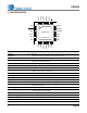
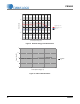
87
6
5
4
3
2
1
9
10
11 12
19
2021222324
13
14
15
16
17
18
Top-Down (Through Package) View
24-Pin QFN Package
XOUT
VDDD
GNDD
MODE
SSEL
CS
IIN2-
IIN2+
VREF-
VREF+
GNDA
XIN
RESET
IIN1-
IIN1+
VIN+
SCLK
RX/SDI
TX/SDO
DO2
DO1
Thermal Pad
VIN-
VDDA
DO3