
User guide

CS5480
42 DS980F3
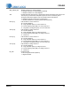
6.6.4 Phase Compensation (PC) – Page 0, Address 5
Default = 0x00 0000
CPCC2[1:0] Coarse phase compensation control for I2 and V2.
00 = No extra delay
01 = 1 OWR delay in current channel 2
10 = 1 OWR delay in voltage channel 2
11 = 2 OWR delay in voltage channel 2
CPCC1[1:0] Coarse phase compensation control for I1 and V1.
00 = No extra delay
01 = 1 OWR delay in current channel 1
10 = 1 OWR delay in voltage channel 1
11 = 2 OWR delay in voltage channel 1
[19:18] Reserved.
FPCC2[8:0] Fine phase compensation control for I2 and V2.
Sets a delay in current, relative to voltage.
Resolution: 0.008789° at 50Hz and 0.010547° at 60Hz (OWR = 4000)
FPCC1[8:0] Fine phase compensation control for I1 and V1.
Sets a delay in current, relative to voltage.
Resolution: 0.008789° at 50Hz and 0.010547° at 60Hz (OWR = 4000)
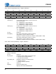
6.6.5 UART Control (SerialCtrl) – Page 0, Address 7
Default = 0x02 004D
[23:19] Reserved.
RX_PU_OFF Disable the pull-up resistor on the RX input pin.
0 = Pull-up resistor enabled (Default)
1 = Pull-up resistor disabled
RX_CSUM_OFF Disable the checksum on serial port data.
0 = Enable checksum
1 = Disable checksum (Default)
[16] Reserved.
BR[15:0] Baud rate (serial bit rate).
BR[15:0] = Baud Ratex524288/MCLK
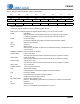
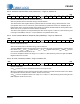
23 22 21 20 19 18 17 16
CPCC2[1] CPCC2[0] CPCC1[1] CPCC1[0] - - FPCC2[8] FPCC2[7]
15 14 13 12 11 10 9 8
FPCC2[6] FPCC2[5] FPCC2[4] FPCC2[3] FPCC2[2] FPCC2[1] FPCC2[0] FPCC1[8]
76543210
FPCC1[7] FPCC1[6] FPCC1[5] FPCC1[4] FPCC1[3] FPCC1[2] FPCC1[1] FPCC1[0]
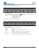
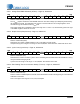
23 22 21 20 19 18 17 16
- - - - - RX_PU_OFF RX_CSUM_OFF -
15 14 13 12 11 10 9 8
BR[15] BR[14] BR[13] BR[12] BR[11] BR[10] BR[9] BR[8]
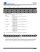
765432 10
BR[7] BR[6] BR[5] BR[4] BR[3] BR[2] BR[1] BR[0]