
User guide

CS5480
DS980F3 25
5.6.1.2 Manual Channel Selection
In addition to automatic channel selection anti-tamper-
ing scheme, the CS5480 allows the user or application
program to select the more appropriate energy channel
manually. Configuration 2 (Config2) register bit IHOLD
disable automatic channel selection, and ICHAN forces
the selection of the contributor to the total power regis-
ters (see Figure 14).
5.6.2 Anti-tampering on Voltage
An internal RMS voltage reference is also available in
the event that the voltage input has been compromised
by tampering.
If the user application detects the voltage input has
been impaired, it may choose to use the fixed internal
RMS voltage reference in active power calculations by
setting the VFIX bit in the Configuration 2 (Config2) reg-
ister. The value of the Voltage Fixed RMS Reference
(VF
RMS
) register is by default 0.707107 (full-scale RMS)
but can be changed by the application program. Figure
14 shows the entry point for the VF
RMS
value. VF
RMS
has no phase relationship to I1
RMS
or I2
RMS
. Therefore,
the VF
RMS
only affects the active power calculation
paths.
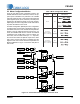
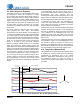
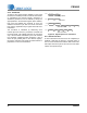
5.7 Energy Pulse Generation
The CS5480 provides three independent energy pulse
generation blocks (EPG1, EPG2, and EPG3) in order to
simultaneously output active, reactive, and apparent
energy pulses on any of the three digital output pins
(DO1, DO2, and DO3). The energy pulse frequency is
proportional to the magnitude of the power. The energy
pulse output is commonly used as the test output of a
power meter.
The host microcontroller can also use the
energy pulses to accumulate the energy
(see Figure 16)
.
P
SUM
Sign
Q
SUM
Sign
P1 Sign
P2 Sign
Q1 Sign
Q2 Sign
DO1_OD
(Config1)
DO2_OD
(Config1)
DO3_OD
(Config1)
(PulseCtrl) EPGxIN[3:0]
DOxMODE[3:0]
(Config1)
DO3
DO2
DO1
Hi-Z
Interrupt
P
SUM
Q
SUM
S
SUM
P1
AVG
P2
AVG
Q1
AVG
Q2
AVG
S1
AVG
S2
AVG
PULSE RATE
EPGx_ON
(Config1)
MCLK
(PulseWidth) PW[7:0]
(PulseWidth) FREQ_RNG[3:0]
0000
0001
0010
0011
0100
0101
0110
0111
1000
Energy Pulse Generation (EPG1)
Energy Pulse Generation (EPG2)
Ener gy Pulse Generation (EPG3)
4
4
8
4
Digital Output Mux (DO3)
Digital Output Mux (DO2)
0000
0001
0010
0011
0100
0101
0110
0111
1000
1001
1010
1011
1100
1101
1110
1111
Digital Output Mux (DO1)
RESERVED
RESERVED
RESERVED
V1/V2 Crossing
I1/I2 Crossing
Figure 16. Energy Pulse Generation and Digital Output Control