
User guide

CS5480
DS980F3 13
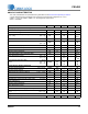
DIGITAL CHARACTERISTICS
• Min / Max characteristics and specifications are guaranteed over all Recommended Operating Conditions.
• Typical characteristics and specifications are measured at nominal supply voltages and T
A
= 25°C.
• VDDA = +3.3V ±10%; GNDA = GNDD = 0V. All voltages with respect to 0V.
• MCLK = 4.096MHz.
Notes: 11. All measurements performed under static conditions.
12. XOUT pin used for crystal only. Typical drive current<1mA.
Parameter Symbol Min Typ Max Unit
Master Clock Characteristics
XIN Clock Frequency
Internal Gate Oscillator MCLK 2.5 4.096 5 MHz
XIN Clock Duty Cycle 40 - 60 %
Filter Characteristics
Phase Compensation Range
(60Hz, OWR = 4000Hz) -10.79 - +10.79 °
Input Sampling Rate - MCLK/8 - Hz
Digital Filter Output Word Rate
(Both channels) OWR - MCLK/1024 - Hz
High-pass Filter Corner Frequency
-3dB -2.0-Hz
Input/Output Characteristics
High-level Input Voltage (All Pins) V
IH
0.6(VDDA) - - V
Low-level Input Voltage (All Pins) V
IL
--0.6V
High-level Output Voltage
DO1-DO3, I
out
=+10mA
(Note 12) All Other Outputs, I
out
=+5mA
V
OH
VDDA-0.3
VDDA-0.3
-
-
-
-
V
V
Low-level Output Voltage
DO1-DO3, I
out
=-12mA
(Note 12) All Other Outputs, I
out
=-5mA
V
OL
-
-
-
-
0.5
0.5
V
V
Input Leakage Current I
in
-±1±10µA
3-state Leakage Current I
OZ
--±10µA
Digital Output Pin Capacitance C
out
-5-pF