CS5480 Three Channel Energy Measurement IC Features Description • The CS5480 is a high-accuracy, three-channel, energy measurement analog front end. • • • • • • • • • • • • • • • • • Superior Analog Performance with Ultra-low Noise Level & High SNR Energy Measurement Accuracy of 0.1% over 4000:1 Dynamic Range Current RMS Measurement Accuracy of 0.
CS5480 TABLE OF CONTENTS 1. Overview . . . . . . . . . . . . . . . . . . . . . . . . . . . . . . . . . . . . . . . . . . . . . . . . . . . . . . . . . . . . . . . .5 2. Pin Description . . . . . . . . . . . . . . . . . . . . . . . . . . . . . . . . . . . . . . . . . . . . . . . . . . . . . . . . . . .6 2.1 Analog Pins . . . . . . . . . . . . . . . . . . . . . . . . . . . . . . . . . . . . . . . . . . . . . . . . . . . . . . . .7 2.1.1 Voltage Input . . . . . . . . . . . . . . . . . . . . . . . . . . . . . .
CS5480 5.7.1 Pulse Rate . . . . . . . . . . . . . . . . . . . . . . . . . . . . . . . . . . . . . . . . . . . . . . . . . . 26 5.7.2 Pulse Width . . . . . . . . . . . . . . . . . . . . . . . . . . . . . . . . . . . . . . . . . . . . . . . . . . 26 5.8 Voltage Sag, Voltage Swell, and Overcurrent Detection . . . . . . . . . . . . . . . . . . . . . 26 5.9 Phase Sequence Detection . . . . . . . . . . . . . . . . . . . . . . . . . . . . . . . . . . . . . . . . . . . 27 5.10 Temperature Measurement . . . . . . .
CS5480 LIST OF FIGURES Figure 1. Oscillator Connections................................................................................................... 7 Figure 2. Multi-device UART Connections.................................................................................... 8 Figure 3. UART Serial Frame Format ........................................................................................... 8 Figure 4. Active Energy Load Performance............................................................
CS5480 1. OVERVIEW The CS5480 is a CMOS power measurement integrated circuit that uses three analog-to-digital converters to measure line voltage, two currents and temperature. It calculates active, reactive, and apparent power as well as RMS voltage and current and peak voltage and current. It handles other system-related functions, such as energy pulse generation, voltage sag and swell, overcurrent and zero-crossing detection, and line frequency measurement.
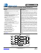
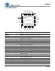
CS5480 XOUT VDDD GNDD MODE SSEL CS 2. PIN DESCRIPTION 24 23 22 21 20 19 XIN 1 18 SCLK RESET 2 17 RX/SDI IIN1- 3 16 TX/SDO IIN1+ 4 15 DO3 VIN+ 5 14 DO2 VIN- 6 13 DO1 Thermal Pad 7 8 9 10 11 12 IIN2- IIN2+ VREF- VREF+ GNDA VDDA Top-Down (Through Package) View 24-Pin QFN Package Clock Generator Crystal In Crystal Out 1,24 XIN, XOUT — Connect to an external quartz crystal.
CS5480 2.1 Analog Pins The CS5480 has a differential input (VIN) for voltage input and two differential inputs IIN1 IIN2) for current1 and current2 inputs. The CS5480 also has two voltage reference pins (VREF) between which a bypass capacitor should be placed. XIN XOUT 2.1.1 Voltage Input The output of the line voltage resistive divider or transformer is connected to the (VIN) input of the CS5480. The voltage channel is equipped with a 10x, fixed-gain amplifier.
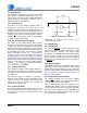
CS5480 2.2.3.1 SPI The CS5480 provides a Serial Peripheral Interface (SPI) that operates as a slave device in 4-wire mode and supports multiple slaves on the SPI bus. The 4-wire SPI includes CS, SCLK, SDI, and SDO signals. SLAVE 0 UART MASTER CS is the chip select input for the CS5480 SPI port. A high logic level de-asserts it, tri-stating the SDO pin and clearing the SPI interface. A low logic level enables the SPI port.
CS5480 3. CHARACTERISTICS AND SPECIFICATIONS RECOMMENDED OPERATING CONDITIONS Parameter Positive Analog Power Supply Specified Temperature Range Symbol VDDA TA Min 3.0 -40 Typ 3.3 - Max 3.6 +85 Unit V °C POWER MEASUREMENT CHARACTERISTICS Parameter Active Energy (Note 1 and 2) Reactive Energy (Note 1 and 2) Apparent Power (Note 1 and 3) Current RMS (Note 1, 3, and 4) Symbol Min Typ Max Unit All Gain Ranges Current Channel Input Signal Dynamic Range 4000:1 PAvg - ±0.
CS5480 1 Percent Error (%) 0.5 0 Lagging sin(੮) = 0.5 Leading sin(੮) = 0.5 sin(੮) = 1 -0.5 -1 0 500 1000 1500 2000 2500 3000 3500 4000 4500 Current Dynamic Range (x : 1) Figure 5. Reactive Energy Load Performance 1 Percent Error (%) 0.5 0 IRMS Error IRMS Error -0.5 -1 0 500 1000 1500 Current Dynamic range (x : 1) Figure 6.
CS5480 ANALOG CHARACTERISTICS • • • • Min / Max characteristics and specifications are guaranteed over all Recommended Operating Conditions. Typical characteristics and specifications are measured at nominal supply voltages and TA = 25°C. VDDA = +3.3V ±10%; GNDA = GNDD = 0V. All voltages with respect to 0V. MCLK = 4.096MHz. Parameter Symbol Min Typ Max Unit CMRR 80 - - dB -0.
CS5480 Parameter Symbol Min Typ Max Unit PSCA - 3.9 - mA PC - 12.9 4.5 - mW mW Power Supplies Power Supply Currents (Active State) IA+ (VDDA = +3.3V) Power Consumption (Note 5) Notes: Active State (VDDA = +3.3V) Stand-by State 5. 6. 7. All outputs unloaded. All inputs CMOS level. Temperature accuracy measured after calibration is performed. Measurement method for PSRR: VDDA = +3.3V, a 150mV (zero-to-peak) (60Hz) sine wave is imposed onto the +3.3V DC supply voltage at the VDDA pin.
CS5480 DIGITAL CHARACTERISTICS • • • • Min / Max characteristics and specifications are guaranteed over all Recommended Operating Conditions. Typical characteristics and specifications are measured at nominal supply voltages and TA = 25°C. VDDA = +3.3V ±10%; GNDA = GNDD = 0V. All voltages with respect to 0V. MCLK = 4.096MHz.
CS5480 SWITCHING CHARACTERISTICS • • • • Min / Max characteristics and specifications are guaranteed over all Recommended Operating Conditions. Typical characteristics and specifications are measured at nominal supply voltages and TA = 25°C. VDDA = +3.3V ±10%; GNDA = GNDD = 0V. All voltages with respect to 0V. Logic Levels: Logic 0 = 0V, Logic 1 = VDDA. Parameter Symbol Min Typ Max Unit DO1-DO3 Any Digital Output Except DO1-DO3 trise - 50 1.
CS5480 CS t6 t1 t3 SCLK t2 t7 SDO MSB t4 SDI t8 MSB-1 LSB INTERMEDIATE BITS t5 MSB MSB-1 INTERMEDIATE BITS LSB Figure 7. SPI Data and Clock Timing CS t10 t9 TX RX START IDLE START LSB DATA MSB STOP IDLE LSB DATA MSB OPTIONAL OVERLAP INSTRUCTION * t11 IDLE STOP STOP * Reading registers during the optional overlap instruction requires the start to occur during the last byte transmitted by the part Figure 8.
CS5480 ABSOLUTE MAXIMUM RATINGS Parameter DC Power Supplies Input Current (Note 16) (Notes 17 and 18) Input Current for Power Supplies Symbol Min Typ Max Unit VDDA -0.3 - +4.0 V IIN - - ±10 mA - - - ±50 - Output Current (Note 19) IOUT - - 100 mA Power Dissipation (Note 20) PD - - 500 mW Input Voltage (Note 21) VIN - 0.3 - (VDDA) + 0.
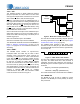
MUX CS5480 PMF DELAY CTRL From V Channel ADC IIR SINC3 V2 HPF Phase Shift V2DCOFF ... CPCC2[1:0] ... FPCC2[8:0] ... SYSGAIN Config 2 I2 DCOFF IIN2± 4th Order Modulator PGA DELAY CTRL Epsilon ... I2FLT[1:0] ... 2 P2 I2 GAIN IIR SINC3 V2FLT[1:0] HPF INT MUX PC V2GAIN Q2 PMF I2 Registers Figure 9. Signal Flow for V1, I1, P1, Q1 Measurements 4. SIGNAL FLOW DESCRIPTION The signal flow consists of two current channels and a voltage channel.
CS5480 4.4 Phase Compensation Phase compensation changes the phase of voltage relative to current by adding a delay in the decimation filters. The amount of phase shift is set by the PC register bits CPCCx[1:0] and FPCCx[8:0] for current channels. For voltage channels, only bits CPCCx[1:0] affect the delay. applied to the other channel to match the phase response of the HPF. For AC power measurement, high-pass filters should be enabled on the voltage and current channels.
CS5480 4.8.1 Fixed Number of Samples Averaging 4.8.5 Reactive Power N is the preset value in the SampleCount register and should not be set less than 100. By default, the SampleCount is 4000. With MCLK = 4.096MHz, the averaging period is fixed at N/4000 = 1 second, regardless of the line frequency.
CS5480 These offsets can be either positive or negative, indicating crosstalk coupling either in phase or out of phase with the applied voltage input. The power offset registers can compensate for either condition. power line. Residual reactive power offsets are usually caused by crosstalk into current channels from voltage channels, or from ripple on the meter’s or chip’s power supply, or from inductance from a nearby transformer. To use this feature, measure the average power at no load.
CS5480 5. FUNCTIONAL DESCRIPTION Table 1. POR Thresholds Typical POR Threshold 5.1 Power-on Reset The CS5480 has an internal power supply supervisor circuit that monitors the VDDA and VDDD power supplies and provides the master reset to the chip. If any of these voltages are in the reset range, the master reset is triggered. The CS5480 has dedicated power-on reset (POR) circuits for the analog supply and digital supply.
CS5480 V(t), I(t) If |VPEAK| > VZXLEVEL, then voltage zero-crossing detection is enabled. If |IPEAK| > IZXLEVEL, then current zero-crossing detection is enabled. If |VPEAK| VZXLEVEL, then voltage zero-crossing detection is disabled. If |IPEAK| IZXLEVEL, then current zero-crossing detection is disabled. VZXLEVEL IZXLEVEL t DOx Zero-crossing output on DOx pin Pulse width = 250μs t Figure 13. Zero-crossing Level and Zero-crossing Output on DOx 5.
CS5480 5.5 Meter Configuration Modes Table 2. Meter Configuration Modes There are two distinct meter configuration modes in the CS5480 that affect how the total active, reactive, and apparent power calculations are performed. The CS5480 has power results for each current channel as well as total power registers (PSUM, QSUM, and SSUM). The total power registers are calculated from either one or both channels, depending on the meter configuration modes. See Table 2 for power calculations in each mode.
CS5480 5.6 Tamper Detection and Correction 5.6.1.1 Automatic Channel Selection In the 1V-1I-1N meter configuration mode, the CS5480 provides flexibility for the user and application program to adjust the anti-tampering scheme automatically or manually. Automatic channel selection is enabled by default. For manual channel selection refer to section 5.6.1.2 Manual Channel Selection on page 25. Automatic channel selection is standard in the CS5480.
CS5480 5.6.1.2 Manual Channel Selection In addition to automatic channel selection anti-tampering scheme, the CS5480 allows the user or application program to select the more appropriate energy channel manually. Configuration 2 (Config2) register bit IHOLD disable automatic channel selection, and ICHAN forces the selection of the contributor to the total power registers (see Figure 14). 5.6.
CS5480 After reset, all three energy pulse generation blocks are disabled (DOxMODE[3:0] = Hi-Z). To output a desired energy pulse to a DOx pin, follow the steps below: 1. Write to register PulseWidth (page 0, address 8) to select the energy pulse width and pulse frequency range. 2. Write to register PulseRate (page 18, address 28) to select the energy pulse rate. 3. Write to register PulseCtrl (page 0, address 9) to select the input to each energy pulse generation block. 4.
CS5480 5.9 Phase Sequence Detection Polyphase meters using multiple CS5480 devices may be configured to sense the succession of voltage zero-crossings and determine which phase order is in service. The phase sequence detection within CS5480 involves counting the number of OWR samples from a starting point to the next voltage zero-crossing rising edge or falling for each phase.
CS5480 Write 0x16 to PSDC Register Start on the Falling Edge on the RX Pin Phase A Channel Stop 2 Phase A Count 0 -2 C Phase B Channel Stop 2 Phase B Count 0 -2 A B Phase C Channel Stop 2 Phase C Count 0 -2 Figure 19. Phase Sequence C, B, A for Rising Edge Transition be write-protected from the serial interface. Setting the The application program can change both the scale and HOST_LCK[4:0] bits to 0x09 disables the range of temperature by changing the Temperature write-protection mode.
CS5480 6. HOST COMMANDS AND REGISTERS 6.1 Host Commands The first byte sent to the CS5480 SDI/RX pin contains the host command. Four types of host commands are required to read and write registers and instruct the calculation engine. The two most significant bits (MSBs) of the host command defines the function to be performed. The following table depicts the types of commands. A register write command is designated by setting the two MSBs of the command to binary ‘01’.
CS5480 6.1.3 Checksum To improve the communication reliability on the serial interface, the CS5480 provides a checksum mechanism on transmitted and received signals. Checksum is disabled by default but can be enabled by setting the appropriate bit in the SerialCtrl register. When enabled, both host and CS5480 are expected to send one additional checksum byte after the normal command byte and the applicable 3-byte register data has been transmitted.
CS5480 6.
CS5480 51 52 53 54 55 56 57 58 59 60 61 62 63 Notes: 32 11 0011 11 0100 11 0101 11 0110 11 0111 11 1000 11 1001 11 1010 11 1011 11 1100 11 1101 11 1110 11 1111 ZXNUM - Reserved Reserved Reserved Reserved Num. Zero Crosses used for Line Freq. Y Reserved Reserved Reserved Reserved Reserved Reserved Reserved Reserved Y 0x 00 0064 - (1) Warning: Do not write to unpublished or reserved register locations. (2) * Registers with checksum protection.
CS5480 6.
CS5480 51** 52 53 54* 55* 56* 57 58* 59* 60* 61 62 63 Notes: 11 0011 11 0100 11 0101 11 0110 11 0111 11 1000 11 1001 11 1010 11 1011 11 1100 11 1101 11 1110 11 1111 SampleCount TGAIN TOFF PMIN (IRMSMIN) TSETTLE LoadMIN VFRMS SYSGAIN Time - Sample Count Reserved Reserved Temperature Gain Temperature Offset Channel Select Minimum Amplitude Filter Settling Time to Conv.
CS5480 6.
CS5480 6.
CS5480 6.6 Register Descriptions 22. “Default” = bit states after power-on or reset 23. DO NOT write a “1” to any unpublished register bit or to a bit published as “0”. 24. DO NOT write a “0” to any bit published as “1”. 25. DO NOT write to any unpublished register address. 6.6.
CS5480 6.6.2 Configuration 1 (Config1) – Page 0, Address 1 23 0 22 EPG3_ON 21 EPG2_ON 20 EPG1_ON 15 1 14 1 13 1 12 0 19 0 18 DO3_OD 17 DO2_OD 16 DO1_OD 11 10 9 8 DO3MODE[3] DO3MODE[2] DO3MODE[1] DO3MODE[0] 7 6 5 4 3 2 1 0 DO2MODE[3] DO2MODE[2] DO2MODE[1] DO2MODE[0] DO1MODE[3] DO1MODE[2] DO1MODE[1] DO1MODE[0] Default = 0x00 EEEE 38 [23] Reserved. EPG3_ON Enable EPG3 block.
CS5480 DO2MODE[3:0] Output control for DO2 pin. 0000 = Energy pulse generation block 1 (EPG1) output 0001 = Energy pulse generation block 2 (EPG2) output 0010 = Energy pulse generation block 3 (EPG3) output 0011 = Reserved 0100 = P1 sign 0101 = P2 sign 0110 = PSUM sign 0111 = Q1 sign 1000 = Q2 sign 1001 = QSUM sign 1010 = Reserved 1011 = V1/V2 zero-crossing 1100 = I1/I2 zero-crossing 1101 = Reserved 1110 = Hi-Z, pin not driven (Default) 1111 = Interrupt DO1MODE[3:0] Output control for DO1 pin.
CS5480 6.6.3 Configuration 2 (Config2) – Page 16, Address 0 23 VFIX 22 POS 21 ICHAN 20 IHOLD 19 IVSP 18 MCFG[1] 17 MCFG[0] 16 - 15 - 14 APCM 13 - 12 ZX_LPF 11 AVG_MODE 10 REG_CSUM_OFF 9 AFC 8 I2FLT[1] 7 I2FLT[0] 6 V2FLT[1] 5 V2FLT[0] 4 I1FLT[1] 3 I1FLT[0] 2 V1FLT[1] 1 V1FLT[0] 0 IIR_OFF Default = 0x00 0200 VFIX Use internal RMS voltage reference instead of voltage input for average active power. 0 = Use voltage input. (Default) 1 = Use internal RMS voltage reference (VFRMS).
CS5480 REG_CSUM_OFF Disable checksum on critical registers. 0 = Enable checksum on critical registers (Default) 1 = Disable checksum on critical registers AFC Enables automatic line frequency measurement which sets Epsilon every time a new line frequency measurement completes. Epsilon is used to control the gain of 90-degree phase shift integrator used in quadrature power calculations.
CS5480 6.6.4 Phase Compensation (PC) – Page 0, Address 5 23 CPCC2[1] 22 CPCC2[0] 21 CPCC1[1] 20 CPCC1[0] 19 - 18 - 17 FPCC2[8] 16 FPCC2[7] 15 FPCC2[6] 14 FPCC2[5] 13 FPCC2[4] 12 FPCC2[3] 11 FPCC2[2] 10 FPCC2[1] 9 FPCC2[0] 8 FPCC1[8] 7 6 5 4 3 2 1 0 FPCC1[7] FPCC1[6] FPCC1[5] FPCC1[4] FPCC1[3] FPCC1[2] FPCC1[1] FPCC1[0] Default = 0x00 0000 CPCC2[1:0] Coarse phase compensation control for I2 and V2.
CS5480 6.6.6 Pulse Output Width (PulseWidth) – Page 0, Address 8 23 - 22 - 21 - 20 - 19 18 17 16 FREQ_RNG[3] FREQ_RNG[2] FREQ_RNG[1] FREQ_RNG[0] 15 PW[15] 14 PW[14] 13 PW[13] 12 PW[12] 11 PW[11] 10 PW[10] 9 PW[9] 8 PW[8] 7 6 5 4 3 2 1 0 PW[7] PW[6] PW[5] PW[4] PW[3] PW[2] PW[1] PW[0] Default = 0x00 0001 (265.6µs at OWR = 4kHz) PulseWidth sets the energy pulse frequency range and the duration of energy pulses.
CS5480 6.6.9 Pulse Output Control (PulseCtrl) – Page 0, Address 9 23 - 22 - 21 - 20 - 19 - 18 - 17 - 16 - 15 - 14 - 13 - 12 - 11 EPG3IN[3] 10 EPG3IN[2] 9 EPG3IN[1] 8 EPG3IN[0] 7 6 5 4 3 2 1 0 EPG2IN[3] EPG2IN[2] EPG2IN[1] EPG2IN[0] EPG1IN[3] EPG1IN[2] EPG1IN[1] EPG1IN[0] Default = 0x00 0000 This register controls the input to the energy pulse generation block (EPGx). [23:12] Reserved. EPGxIN[3:0] Selects the input to the energy pulse generation block (EPGx).
CS5480 6.6.11 Phase Sequence Detection and Control (PSDC) – Page 0, Address 48 23 DONE 22 PSCNT[6] 21 PSCNT[5] 20 PSCNT[4] 19 PSCNT[3] 18 PSCNT[2] 17 PSCNT[1] 16 PSCNT[0] 15 - 14 - 13 - 12 - 11 - 10 - 9 - 8 - 7 - 6 - 5 DIR 4 CODE[4] 3 CODE[3] 2 CODE[2] 1 CODE[1] 0 CODE[0] Default = 0x00 0000 DONE Indicates valid count values reside in PSCNT[6:0]. 0 = Invalid values in PSCNT[6:0]. (Default) 1 = Valid values in PSCNT[6:0].
CS5480 6.6.13 Interrupt Status (Status0) – Page 0, Address 23 23 DRDY 22 CRDY 21 WOF 20 - 19 - 18 MIPS 17 V2SWELL 16 V1SWELL 15 P2OR 14 P1OR 13 I2OR 12 I1OR 11 V2OR 10 V1OR 9 I2OC 8 I1OC 7 V2SAG 6 V1SAG 5 TUP 4 FUP 3 IC 2 RX_CSUM_ERR 1 - 0 RX_TO Default = 0x80 0000 The Status0 register indicates a variety of conditions within the chip. Writing a one to a Status0 register bit will clear that bit. Writing a ‘0’ to any bit has no effect. DRDY Data Ready.
CS5480 6.6.14 Interrupt Mask (Mask) – Page 0, Address 3 23 DRDY 22 CRDY 21 WOF 20 - 19 - 18 MIPS 17 V2SWELL 16 V1SWELL 15 P2OR 14 P1OR 13 I2OR 12 I1OR 11 V2OR 10 V1OR 9 I2OC 8 I1OC 7 V2SAG 6 V1SAG 5 TUP 4 FUP 3 IC 2 RX_CSUM_ERR 1 - 0 RX_TO Default = 0x00 0000 The Mask register is used to control the activation of the INT pin. Writing a '1' to a Mask register bit will allow the corresponding Status0 register bit to activate the INT pin when set.
CS5480 6.6.16 Chip Status 2 (Status2) – Page 0, Address 25 23 - 22 - 21 - 20 - 19 - 18 - 17 - 16 - 15 - 14 - 13 - 12 - 11 - 10 - 9 - 8 - 7 - 6 - 5 QSUM_SIGN 4 Q2_SIGN 3 Q1_SIGN 2 PSUM_SIGN 1 P2_SIGN 0 P1_SIGN Default = 0x00 0000 This register indicates a variety of conditions within the chip. [23:6] Reserved. QSUM_SIGN Indicates the sign of the value contained in QSUM. 0 = positive value 1 = negative value Q2_SIGN Indicates the sign of the value contained in Q2AVG.
CS5480 6.6.18 Automatic Channel Select Level (IchanLEVEL ) – Page 16, Address 50 MSB 20 LSB 2 -1 2 -2 2 -3 2 -4 2 -5 2 -6 2 -7 ..... 2 -17 2 -18 2 -19 2 -20 2 -21 2 -22 2 -23 Default = 0x82 8F5C (1.02 or 2% minimum difference) Sets the hysteresis level for automatic energy channel selection. The channel select level register sets the hysteresis level for automatic energy channel selection.
CS5480 6.6.21 Voltage Fixed RMS Reference (VFRMS ) – Page 16, Address 59 MSB -(20) LSB 2 -1 2 -2 2 -3 2 -4 2 -5 2 -6 2 -7 ..... 2 -17 2 -18 2 -19 2 -20 2 -21 2 -22 2-23 Default = 0x5A 8279 (0.7071068) The VFRMS register contains the internal RMS reference used when voltage input tampering is detected by the application program. The application may choose to set the VFIX bit in the Config2 register to force full-scale energy accumulation at the VFRMS level.
CS5480 6.6.25 System Gain (SysGAIN) – Page 16, Address 60 MSB LSB -(21) 20 2 -1 2 -2 2 -3 2 -4 2 -5 2 -6 ..... 2-16 2-17 2-18 2-19 2-20 2-21 2-22 Default = 0x50 0000 (1.25) System Gain (SysGAIN) is applied to all channels. By default, SysGAIN = 1.25, but can be finely adjusted to compensate for voltage reference error. It is a two's complement value in the range of -2.0value2.0, with the binary point to the right of the second MSB. Values should be kept within 5% of 1.25. 6.6.
CS5480 6.6.29 Voltage 1 Sag Level (V1SagLEVEL ) – Page 17, Address 1 MSB -(20) LSB 2 -1 2 -2 2 -3 2 -4 2 -5 2 -6 2 -7 ..... 2 -17 2 -18 2 -19 2 -20 2 -21 2 -22 2 -23 Default = 0x00 0000 Voltage 1 Sag Level, V1SagLEVEL, establishes a threshold at which a sag event is triggered. This is a two's complement value in the range of -1.0value 1.0, with the binary point to the right of the MSB. Negative values are not used. 6.6.
CS5480 6.6.34 Current 2 Overcurrent Duration (I2OverDUR ) – Page 17, Address 12 MSB 0 LSB 2 22 2 21 220 219 218 217 216 ..... 26 25 24 23 22 21 20 Default = 0x00 0000 Current 2 Overcurrent Duration, I2OverDUR, determines the count of OWR samples utilized to determine an overcurrent event. These are integers in the range of 0 to 8,388,607 samples. A value of zero disables the feature. 6.6.
CS5480 6.6.39 Voltage 2 Swell Level (V2SwellLEVEL ) – Page 18, Address 51 MSB -(20) LSB 2-1 2-2 2-3 2-4 2-5 2-6 2-7 ..... 2-17 2-18 2-19 2-20 2-21 2-22 2-23 Default = 0x7F FFFF Voltage 2 Swell Level, V2SwellLEVEL, establishes a threshold at which a swell event is triggered. This is a two's complement value in the range of -1.0value1.0, with the binary point to the right of the MSB. Negative values are not used. 6.6.
CS5480 6.6.44 RMS Current 1 (I1RMS ) – Page 16, Address 6 MSB 2-1 LSB 2-2 2-3 2-4 2-5 2-6 2-7 2-8 ..... 2-18 2-19 2-20 2-21 2-22 2-23 2-24 Default = 0x00 0000 I1RMS contains the root mean square (RMS) values of I1, calculated during each low-rate interval. This is an unsigned value in the range of 0value1.0, with the binary point to the left of the MSB. 6.6.45 RMS Voltage 1 (V1RMS ) – Page 16, Address 7 MSB 2-1 LSB 2-2 2-3 2-4 2-5 2-6 2-7 2-8 .....
CS5480 6.6.49 Active Power 2 (P2AVG ) – Page 16, Address 11 MSB -(20) LSB 2-1 2-2 2-3 2-4 2-5 2-6 2-7 ..... 2-17 2-18 2-19 2-20 2-21 2-22 2-23 Default = 0x00 0000 Instantaneous power is averaged over each low-rate interval (SampleCount samples) to compute active power (P2AVG). This is a two's complement value in the range of -1.0value1.0, with the binary point to the right of the MSB. 6.6.50 RMS Current 2 (I2RMS) – Page 16, Address 12 MSB 2-1 LSB 2-2 2-3 2-4 2-5 2-6 2-7 2-8 .....
CS5480 6.6.54 Reactive Power 2 (Q2Avg ) – Page 16, Address 16 MSB -(20) LSB 2-1 2-2 2-3 2-4 2-5 2-6 2-7 ..... 2-17 2-18 2-19 2-20 2-21 2-22 2-23 Default = 0x00 0000 Reactive power 2 (Q2AVG) is Q2 averaged over each low-rate interval (SampleCount samples). This is a two's complement value in the range of -1.0value1.0, with the binary point to the right of the MSB. 6.6.55 Instantaneous Quadrature Power 2 (Q2) – Page 16, Address 17 MSB -(20) LSB 2-1 2-2 2-3 2-4 2-5 2-6 2-7 .....
CS5480 6.6.59 Power Factor 1 (PF1) – Page 16, Address 21 MSB -(20) LSB 2-1 2-2 2-3 2-4 2-5 2-6 2-7 ..... 2-17 2-18 2-19 2-20 2-21 2-22 2-23 Default = 0x00 0000 Power factor 1 (PF1) is calculated by dividing active power 1 (P1AVG) by apparent power 1 (S1). The sign is determined by the active power (P1AVG) sign. This is a two's complement value in the range of -1.0value1.0, with the binary point to the right of the MSB. 6.6.
CS5480 6.6.64 Temperature (T) – Page 16, Address 27 MSB LSB -(27) 26 25 24 23 22 21 20 ..... 2-10 2-11 2-12 2-13 2-14 2-15 2-16 Default = 0x00 0000 T contains results from the on-chip temperature measurement. By default, T uses the Celsius scale, and is a two's complement value in the range of -128.0value128.0 (°C), with the binary point to the right of bit 16. Negative values are not used. T can be rescaled by the application using the TGAIN and TOFF registers. 6.6.
CS5480 6.6.68 DC Offset for Current (I1DCOFF , I2DCOFF ) – Page 16, Address 32, 39 MSB -(20) LSB 2-1 2-2 2-3 2-4 2-5 2-6 2-7 ..... 2-17 2-18 2-19 2-20 2-21 2-22 2-23 Default = 0x00 0000 DC offset registers I1DCOFF and I2DCOFF are initialized to zero on reset. During DC offset calibration, selected registers are written with the inverse of the DC offset measured. The application program can also write the DC offset register values. These are two's complement values in the range of -1.
CS5480 6.6.73 Average Reactive Power Offset (Q1OFF , Q2OFF ) – Page 16, Address 38, 45 MSB -(20) LSB 2-1 2-2 2-3 2-4 2-5 2-6 2-7 ..... 2-17 2-18 2-19 2-20 2-21 2-22 2-23 Default = 0x00 0000 Average Reactive Power Offset (Q1OFF , Q2OFF ) is added to averaged reactive power to yield Q1AVG (Q2AVG ) register results. It can be used to reduce systematic energy errors. These are two's complement values in the range of -1.0 value 1.0, with the binary point to the right of the MSB. 6.6.
CS5480 6.6.77 Calibration Scale (Scale) – Page18, Address 63 MSB -(20) LSB 2-1 2-2 2-3 2-4 2-5 2-6 2-7 ..... 2-17 2-18 2-19 2-20 2-21 2-22 2-23 Default = 0x4C CCCC (0.6) The Scale register is used in the gain calibration to set the level of calibrated results of I-channel RMS. During gain calibration, the IxRMS results register is divided into the Scale register. The quotient is put into the IxGAIN register. This is a two's complement value in the range of -1.0value1.
CS5480 7. SYSTEM CALIBRATION procedure takes the time of N +TSETTLE OWR samples. As N is increased, the calibration takes more time but the accuracy of calibration results tends to increase. Component tolerances, residual ADC offset, and system noise require a meter to be calibrated before it meets a specific accuracy requirement. The CS5480 provides an on-chip calibration algorithm to operate the system calibration quickly and easily.
CS5480 The AC offset register for the channel being calibrated should first be cleared prior to performing the calibration. The high-pass filter should be enabled if AC offset calibration is used. It is recommended that TSETTLE be set to 2000ms before performing an AC offset calibration. Note that the AC offset register holds the square of RMS value measured during calibration. Therefore, it can hold a maximum RMS noise of 0xFFFFFF . This is the maximum RMS noise that AC offset correction can remove. 7.1.
CS5480 Once the phase offset is known, the CPCCx and FPCCx bits for that channel are calculated and programmed in the PC register. CPCCx bits are used if either: • • The phase offset is more than 1 output word rate (OWR) sample. More delay is needed on the voltage channel. The compensation resolution is 0.008789° at 50Hz and 0.010547° at 60Hz at an OWR of 4000Hz. 7.
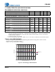
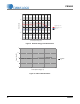
CS5480 8. BASIC APPLICATION CIRCUITS Figure 27 shows the CS5480 configured to measure power in a single-phase, 3-wire system with 1 voltage and 2 currents (1V-2I). Figure 28 shows the CS5480 configured to measure power in a single-phase, 2-wire system with 1 voltage, 1 line current and 1 neutral current (1V-1I-1N). In these diagrams, current transformers (CTs) are used to sense the line load currents, and resistive voltage dividers are used to sense the line voltage. +3.3V L1 N +3.3V 0.1µF 0.
CS5480 +3.3V 0.1µF 0.1µF L N Wh VDDA MODE VDDD VIN + +3.3V Varh +3.3V 27nF SSEL 27nF 1K VIN - +3.3V DO1 5 x 330K 1K DO2 DO3 RX CS5480 ½ R BURDEN 1K CT TX IIN1+ 27nF CS 27nF XIN ½ R BURDEN 1K Interrupt IIN1- 4.096MHz XOUT VREF+ ½ R BURDEN CT 1K IIN227nF 27nF LOA D 0.1 µF VREF- ½ R BURDEN 1K Application Processor IIN2+ +3.3V 10K RESET GNDA GNDD 0. 1µF 1 Voltage , 1 Line Current, and 1 Neutral Current Figure 28.
CS5480 9. PACKAGE DIMENSIONS 24 QFN (4mmX4mm BODY with EXPOSED PAD) PACKAGE DRAWING Dimension A A1 A3 b D D2 e E E2 L aaa bbb ddd eee MIN 0.80 0.00 0.20 2.40 2.40 0.35 mm NOM 0.90 0.02 0.20 REF 0.25 4.00 BSC 2.50 0.50 BSC 4.00 BSC 2.50 0.40 0.15 0.10 0.05 0.08 MAX 1.00 0.05 MIN 0.031 0.000 0.30 0.008 2.60 0.094 2.60 0.45 0.094 0.014 inch NOM 0.035 0.001 0.008 REF 0.010 0.157 BSC 0.098 0.020 BSC 0.157 BSC 0.098 0.016 0.006 0.004 0.002 0.003 MAX 0.039 0.002 0.012 0.102 0.102 0.018 Notes: 1.
CS5480 10. ORDERING INFORMATION Ordering Number Container CS5480-INZ Bulk CS5480-INZR Tape & Reel Temperature Package -40 to +85 °C 24-pin QFN, Lead (Pb) Free 11. ENVIRONMENTAL, MANUFACTURING, AND HANDLING INFORMATION Part Number Peak Reflow Temp MSL Rating* Max Floor Life CS5480-INZ 260 °C 3 7 Days * MSL (Moisture Sensitivity Level) as specified by IPC/JEDEC J-STD-020. 12. REVISION HISTORY Revision Date PP1 APR 2012 Preliminary release. F1 APR 2012 Edited for content and clarity.
CS5480 Contacting Cirrus Logic Support For all product questions and inquiries contact a Cirrus Logic Sales Representative. To find the one nearest to you go to www.cirrus.com IMPORTANT NOTICE Cirrus Logic, Inc. and its subsidiaries (“Cirrus”) believe that the information contained in this document is accurate and reliable. However, the information is subject to change without notice and is provided “AS IS” without warranty of any kind (express or implied).