
Manual


CS5464
DS682F3 13
SWITCHING CHARACTERISTICS (Continued)
Notes: 19. Pulse output timing is specified at DCLK = 4.096 MHz, E2MODE = 0, and E3MODE[1:0] = 0. Refer to
6.7 Energy Pulse Outputs on page 19 for more information on pulse output pins.
20. Timing is proportional to the frequency of DCLK.
ABSOLUTE MAXIMUM RATINGS
WARNING: Operation at or beyond these limits may result in permanent damage to the device.
Normal operation is not guaranteed at these extremes
.
Notes: 21. VA+ and AGND must satisfy [(VA+) - (AGND)] + 6.0 V.
22. VD+ and AGND must satisfy [(VD+) - (AGND)] + 6.0 V.
23. Applies to all pins including continuous over-voltage conditions at the analog input pins.
24. Transient current of up to 100 mA will not cause SCR latch-up.
25. Maximum DC input current for a power supply pin is ±50 mA.
26. Total power dissipation, including all input currents and output currents.
Parameter Symbol Min Typ Max Unit
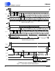
E1
, E2, and E3 Timing (Note 19 and 20)
Period t
period
500 - - s
Pulse Width t
pw
244 - - s
Rising Edge to Falling Edge t
3
6--s
E2
Setup to E1 and/or E3 Falling Edge t
4
1.5 - - s
E1
Falling Edge to E3 Falling Edge t
5
248 - - s
Parameter Symbol Min Typ Max Unit
DC Power Supplies
(Notes 21 and 22)
Positive Digital
Positive Analog
VD+
VA+
-0.3
-0.3
-
-
+6.0
+6.0
V
V
Input Current, Any Pin Except Supplies
(Notes 23, 24, 25) I
IN
--±10mA
Output Current, Any Pin Except VREFOUT I
OUT
--100mA
Power Dissipation
(Note 26) PD --500mW
Analog Input Voltage
All Analog Pins V
INA
- 0.3 - (VA+) + 0.3 V
Digital Input Voltage
All Digital Pins V
IND
-0.3 - (VD+) + 0.3 V
Ambient Operating Temperature T
A
-40 - 85 °C
Storage Temperature T
stg
-65 - 150 °C
t
period
E1
t
3
t
4
t
5
t
3
t
5
t
4
E2
E3
t
pw
t
period
t
pw
Figure 2. Timing Diagram for E1, E2, and E3