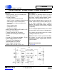
CS5464 Three-channel, Single-phase Power/Energy IC Features & Description Description • Energy Linearity: ±0.1% of Reading over 1000:1 Dynamic Range • On-chip Functions: The CS5464 is a watt-hour meter on a chip. It measures line voltage and current and calculates active, reactive, apparent power, energy, power factor, and RMS voltage and current.
CS5464 TABLE OF CONTENTS 1. Overview . . . . . . . . . . . . . . . . . . . . . . . . . . . . . . . . . . . . . . . . . . . . . . . . . . . . . . . . . . 5 2. Pin Description . . . . . . . . . . . . . . . . . . . . . . . . . . . . . . . . . . . . . . . . . . . . . . . . . . . . . 6 Clock Generator . . . . . . . . . . . . . . . . . . . . . . . . . . . . . . . . . . . . . . . . . . . . . . . . . . . . . . . . . . 6 Control Pins and Serial Data I/O . . . . . . . . . . . . . . . . . . . . . . . . . . . . . . . .
CS5464 5.1.4 Voltage Reference Input . . . . . . . . . . . . . . . . . . . . . . . . . . . . . . . . . . 5.1.5 Voltage Reference Output . . . . . . . . . . . . . . . . . . . . . . . . . . . . . . . . 5.1.6 Crystal Oscillator . . . . . . . . . . . . . . . . . . . . . . . . . . . . . . . . . . . . . . . . 5.2 Digital Pins . . . . . . . . . . . . . . . . . . . . . . . . . . . . . . . . . . . . . . . . . . . . . . . . . . 5.2.1 Reset Input . . . . . . . . . . . . . . . . . . . . . . . . . . . . . . . . . . . .
CS5464 9.1.4 Temperature Sensor Calibration . . . . . . . . . . . . . . . . . . . . . . . . . . . . 9.1.4.1 Temperature Offset Calibration . . . . . . . . . . . . . . . . . . . . . . . 9.1.4.2 Temperature Gain Calibration . . . . . . . . . . . . . . . . . . . . . . . . 10. E2PROM Operation . . . . . . . . . . . . . . . . . . . . . . . . . . . . . . . . . . . . . . . . . . . . . . . 10.1 E2PROM Configuration . . . . . . . . . . . . . . . . . . . . . . . . . . . . . . . . . . . . . . . 10.2 E2PROM Code . . .
CS5464 1. OVERVIEW The CS5464 is a CMOS power measurement integrated circuit utilizing four analog-to-digital converters to measure line voltage, temperature, and current from up to two sources. It calculates active, reactive, and apparent power as well as RMS and peak voltage and current. It handles other system-related functions, such as pulse output conversion, voltage sag, current fault, voltage zero crossing, line frequency, and tamper detection.
CS5464 2.
CS5464 3. CHARACTERISTICS & SPECIFICATIONS RECOMMENDED OPERATING CONDITIONS Parameter Positive Digital Power Supply Positive Analog Power Supply Voltage Reference Specified Temperature Range Symbol VD+ VA+ VREFIN TA Min 3.135 4.75 -40 Typ 5.0 5.0 2.5 - Max 5.25 5.25 +85 Unit V V V °C ANALOG CHARACTERISTICS • • • • Min / Max characteristics and specifications are guaranteed over all Recommended Operating Conditions.
CS5464 ANALOG CHARACTERISTICS (Continued) Parameter Analog Inputs (Voltage Inputs) Differential Input Range Symbol Min Typ Max Unit [(VIN+) – (VIN-)] VIN - 500 - mVP-P Total Harmonic Distortion Crosstalk from Current Inputs at Full Scale (50, 60 Hz) Input Capacitance All Gain Ranges Effective Input Impedance Noise (Referred to Input) THD IC EII NV 65 2 - 75 -70 2.
CS5464 VOLTAGE REFERENCE Parameter Symbol Min Typ Max Unit VREFOUT +2.4 +2.5 +2.6 V Reference Output Output Voltage Temperature Coefficient (Note 8) TCVREF - 40 - ppm/°C Load Regulation (Note 9) VR - 6 10 mV VREFIN +2.4 +2.5 +2.6 V Input Capacitance - 4 - pF Input CVF Current - 100 - nA Reference Input Input Voltage Range Notes: 8. The voltage at VREFOUT is measured across the temperature range.
CS5464 DIGITAL CHARACTERISTICS • • • • Min / Max characteristics and specifications are guaranteed over all Recommended Operating Conditions. Typical characteristics and specifications are measured at nominal supply voltages and TA = 25 °C. VA+ = VD+ = 5V ±5%; AGND = DGND = 0 V. All voltages with respect to 0 V. DCLK = 4.096 MHz.
CS5464 SWITCHING CHARACTERISTICS • • • • Min / Max characteristics and specifications are guaranteed over all Recommended Operating Conditions. Typical characteristics and specifications are measured at nominal supply voltages and TA = 25 °C. VA+ = 5 V ±5% VD+ = 3.3 V ±5% or 5 V ±5%; AGND = DGND = 0 V. All voltages with respect to 0 V. Logic Levels: Logic 0 = 0 V, Logic 1 = VD+. Parameter Symbol Min Typ Max Unit trise - 50 1.0 - µs ns tfall - 50 1.
CS5464 t3 CS t1 t2 SC LK H ig h B y te LSB MSB MSB-1 LSB MSB-1 LSB C o m m a n d T im e 8 S C L K s MSB MSB t5 MSB-1 LSB SDI MSB-1 MSB t4 M id B y te L o w B y te SDI Write Timing (Not to Scale) CS t1 t8 LSB MSB-1 LSB MSB Low B yte MSB-1 LSB UNKNOW N MSB-1 MSB SDO M id B yte MSB H igh B yte t6 t7 t2 LSB MSB-1 SDI MSB SCLK C om m and T im e 8 S C LK s S Y N C 0 or S Y N C 1 C om m and S Y N C 0 or S Y N C 1 C om m and S Y N C 0 or S Y N C 1 C om m and SDO Re
CS5464 SWITCHING CHARACTERISTICS (Continued) Parameter Symbol Min Typ Max Unit tperiod 500 - - s Pulse Width tpw 244 - - s Rising Edge to Falling Edge t3 6 - - s E2 Setup to E1 and/or E3 Falling Edge t4 1.5 - - s E1 Falling Edge to E3 Falling Edge t5 248 - - s E1, E2, and E3 Timing (Note 19 and 20) Period Notes: 19. Pulse output timing is specified at DCLK = 4.096 MHz, E2MODE = 0, and E3MODE[1:0] = 0. Refer to 6.
CS5464 V1OFF V1GAIN FGA I1OFF I1GAIN Figure 3. Signal Flow for V1, I1, P1, Q1 Measurements 4. SIGNAL PATH DESCRIPTION The data flow for voltage and current measurement and the other calculations are shown in Figures 3, 4, and 5. The data flow consists of two current paths and two voltage paths. Both voltage paths are derived from the same differential input pins. Each current path has its own differential input pins. 4.
CS5464 4.4 DC Offset and Gain Correction The system and chip inherently have gain and offset errors which can be removed using the gain and offset registers. (See Section 9. System Calibration on page 39). Each measurement channel has its own registers. For every channel, the output of the IIR filter is added to the offset register and multiplied by the gain register. 4.5 High-pass Filters Optional high-pass filters (HPF in Figures 3 and 4) remove any DC from the selected signal paths.
CS5464 V1ACOFF (V2ACOFF) P1OFF (P2OFF) I1ACOFF (I2ACOFF) Figure 5. Low-rate Calculations 4.8 Power and Energy Results The instantaneous voltage and current samples are multiplied to obtain the instantaneous power (P1, P2) (see Figure 3 and 4). The product is then averaged over N conversions to compute active power (P1AVG, P2AVG).
CS5464 5. PIN DESCRIPTIONS 5.1 Analog Pins 5.1.6 Crystal Oscillator The CS5464 has three differential inputs: VIN IIN1, and IIN2 are the voltage, current1, and current2 inputs, respectively. A single-ended power fail monitor input, voltage reference input, and voltage reference output are also available. An external quartz crystal can be connected to the XIN and XOUT pins as shown in Figure 6. To reduce system cost, each pin is supplied with an on-chip, phase-shifting capacitor to ground. 5.1.
CS5464 5.2.5 Serial Interface The CS5464 provides 5 pins, SCLK, SDI, SDO, CS, and MODE for communication between a host microcontroller or serial E2PROM and the CS5464. MODE is an input that, when high, indicates to the CS5464 that a serial E2PROM is being used instead of a host microcontroller. It has a weak pull-down allowing it to be left unconnected if microcontroller mode is used. SCLK is used to shift and qualify serial data.
CS5464 6. SETTING UP THE CS5464 6.1 Clock Divider The internal clock to the CS5464 needs to operate around 4 MHz. However, by using the internal clock divider, a higher crystal frequency can be used. This is important when driving an external microcontroller requiring a faster clock and using the CPUCLK output. K is the divide ratio from the crystal input to the internal clock and is selected with Configuration register (Config) bits K[3:0]. It has a range of 1 to 16.
CS5464 lists the functions of E3 as controlled by E3MODE[1:0] in the Modes register when E1MODE is not enabled. E3MODE1 E3MODE0 E3 output 0 0 Reactive Energy 0 1 Power Fail Monitor 1 0 Voltage Sign 1 1 Apparent Energy Table 5. E3 Pin Configuration When both E2MODE bits are high, the E1MODE bits are enabled, allowing active, apparent, reactive, or wideband reactive energy for both energy channels to be output on E1 and E2. Table 6 lists the functions of E1 and E2 with E1MODE enabled.
CS5464 For each enabled input channel, the measured value is rectified and compared to the associated level register. Over the duration window, the number of samples above and below the level are counted. If the number of samples below the level exceeds the number of samples above, a Status register bit V1SAG (V2SAG), I1FAULT (I2FAULT) is set, indicating a sag or fault condition. (see Figure 7)..
CS5464 7. USING THE CS5464 7.1 Initialization The CS5464 uses a power-on-reset circuit (POR) to provide an internal reset until the analog voltage reaches 4.0 V. The RESET input pin can also be used by the application circuit to reset the part. After RESET is removed and the oscillator is stable, an initialization program is executed to set the default register values. change. Modes register bit Ichan selects the energy channel, and is normally driven by the CS5464 program.
CS5464 7.4 Command Interface Commands and data are transferred most-significant bit (MSB) first. Figure 1 on page 12, defines the serial port timing. Commands are clocked in on SDI using SCLK. They are a single byte (8 bits) long and fall into one of four basic types: 1. Register Read 2. Register Write 3. Synchronizing 4. Instructions Register reads will cause up to four bytes of register data to be clocked out, MSB first on the SDO pin by SCLK.
CS5464 7.6 Commands All commands are 1 byte (8 bits) long. Many command values are unused and should NOT be written by the application program. All commands except register reads, register writes, or synchronizing commands will abort any conversion, calibration, or any initialization sequence currently executing. This includes reset. No commands other than reads or synchronizing should be executed until the reset sequence completes. 7.6.
CS5464 7.6.4 Calibration B7 1 B6 0 B5 CAL5 B4 CAL4 B3 CAL3 B2 CAL2 B1 CAL1 B0 CAL0 The CS5464 can perform gain and offset calibrations using either DC or AC signals. Proper input levels must be applied to the current inputs and voltage input before performing calibrations.
CS5464 7.6.5 Register Read and Write B7 0 B6 W/R B5 RA4 B4 RA3 B3 RA2 B2 RA1 B1 RA0 B0 0 Read and Write commands provide access to on-chip registers. After a Read command, the addressed data can be clocked out the SDO pin by SCLK. After a Write command, 24 bits of write data must follow. The data is transferred to the addressed register after the 24th data bit is received. Registers are organized into pages of 32 addresses each.
CS5464 Page1 Registers Address 0 1 2 3 4 5 6 7 8 9 10 11 12 13 14 15 16 17 18 19 20 21 22 23 24 25 26 27 28 29 31 W RA[4:0] 00000 00001 00010 00011 00100 00101 00110 00111 01000 01001 01010 01011 01100 01101 01110 01111 10000 10001 10010 10011 10100 10101 10110 10111 11000 11001 11010 11011 11100 11101 11111 Name I1OFF I1GAIN V1OFF V1GAIN P1OFF I1ACOFF V1ACOFF I2OFF I2GAIN V2OFF V2GAIN P2OFF I2ACOFF V2ACOFF PulseWidth PulseRate Modes Epsilon IchanLEVEL N Q1WB Q2WB TGAIN TOFF EMIN (IrmsMIN) TSETTLE LoadMIN
CS5464 8. REGISTER DESCRIPTIONS 1. “Default” = bit states after power-on or reset 2. DO NOT write a “1” to any unpublished register bit. 3. DO NOT write to any unpublished register address. 8.1 Page Register 8.1.1 Page – Address: 31, Write-only, can be written from ANY page. MSB LSB 26 2 5 2 4 2 3 2 2 1 2 20 Default = 0 Register Read and Write commands contain only 5 address bits. But the internal address bus of the CS5464 is 12 bits wide. Therefore, registers are organized into “Pages”.
CS5464 8.2.2 Instantaneous Current (I1, I2), Voltage (V1, V2), and Power (P1, P2) Address: 1 (I1), 2 (V1), 3 (P2), 7 (I2), 8 (V2), 9 (P2) MSB 0 -(2 ) LSB 2 -1 2 -2 -3 2 -4 2 -5 2 -6 2 -7 2 ..... 2-17 2 -18 2 -19 2 -20 2 -21 2 -22 2-23 I1 (I2) and V1 (V2) contain instantaneous current and voltage, respectively, which are multiplied to yield instantaneous power, P1 (P2). These are two's complement values in the range of -1.0 value 1.
CS5464 8.2.7 Peak Current (I1PEAK, I2PEAK ) and Peak Voltage (V1PEAK, V2PEAK ) Address: 18 (I1PEAK), 19 (V1PEAK), 22 (I2PEAK), 23 (V2PEAK) MSB -(20) LSB 2-1 2-2 2-3 2-4 2-5 2-6 2-7 ..... 2-17 2-18 2-19 2-20 2-21 2-22 2-23 Peak current, I1PEAK (I2PEAK) and peak voltage, V1PEAK (V2PEAK) are the instantaneous current and voltage samples with the greatest magnitude detected during the last low-rate interval. These are two's complement values in the range of -1.0 value 1.
CS5464 8.2.12 Internal Status (Status) and Interrupt Mask (Mask) Address: 15 (Status); 26 (Mask) 23 DRDY 22 I2OR 21 V2OR 20 CRDY 19 I2ROR 18 V2ROR 17 I1OR 16 V1OR 15 E2OR 14 I1ROR 13 V1ROR 12 E1OR 11 I1FAULT 10 V1SAG 9 I2FAULT 8 V2SAG 7 TUP 6 TOD 5 I2OD 4 VOD 3 I1OD 2 LSD 1 FUP 0 IC Default = 1 (Status), 0 (Mask) The Status register indicates a variety of conditions within the chip.
CS5464 8.2.13 Control (Ctrl) – Address: 28 23 PC7 22 PC6 21 PC5 20 PC4 19 PC3 18 PC2 17 PC1 16 PC0 15 - 14 - 13 - 12 I2gain 11 - 10 - 9 - 8 STOP 7 - 6 - 5 I1gain 4 INTOD 3 - 2 NOCPU 1 NOOSC 0 - Default = 0 PC[7:0] Phase compensation for channel 2. Sets a delay in voltage relative to current. Phase is signed and in the range of -1.0 value 1.0 sample (OWR) intervals. I1gain (I2gain) Sets the gain of the current1 (current2) input. 0 = Gain is set for ±250mV range.
CS5464 8.3 Page 1 Registers 8.3.1 DC Offset for Current (I1OFF , I2OFF ) and Voltage (V1OFF , V2OFF ) Address: 0 (I1OFF), 2 (V1OFF), 7 (I2OFF), 9 (V2OFF) MSB -(20) LSB 2-1 2-2 2-3 2-4 2-5 2-6 2-7 ..... 2-17 2-18 2-19 2-20 2-21 2-22 2-23 Default = 0 DC offset registers I1OFF & V1OFF (I2OFF & V2OFF) are initialized to zero on reset. During DC offset calibration, selected registers are written with the inverse of the DC offset measured.
CS5464 8.3.5 Mode Control (Modes) – Address: 16 23 Ichan 22 VFIX 21 - 20 - 19 - 18 - 17 - 16 - 15 IvsE 14 E1MODE1 13 E1MODE0 12 Ihold 11 - 10 E2MODE1 9 E2MODE0 8 VHPF2 7 6 5 4 3 2 1 0 IHPF2 VHPF1 IHPF1 - E3MODE1 E3MODE0 POS AFC Default = 0 Ichan Chooses an energy channel to drive the EPULSE, SPULSE, and QPULSE registers. 0 = Pulse registers driven by energy channel 1. 1 = Pulse registers driven by energy channel 2.
CS5464 E3MODE[1:0] E3 Output Mode (with E1MODE enabled) 00 = Power Fail Monitor 01 = Energy Sign 10 = not used 11 = not used POS Positive Energy Only. Suppresses negative values in P1AVG and P2AVG. If a negative value is calculated, zero will be stored instead. AFC Enables automatic line frequency measurement which sets Epsilon every time a new line frequency measurement completes. Epsilon is used to control the gain of the 90 degree phase shift integrator used in quadrature power calculations. 8.3.
CS5464 8.3.9 Cycle Count (N) – Address: 19 MSB LSB 22 0 2 21 2 20 2 19 2 18 2 2 17 2 16 ..... 26 5 2 4 2 3 2 2 2 1 20 2 Default = 4000 Determines the number of output word rate (OWR) samples to use in calculating low-rate results. Cycle Count (N) is an integer in the range of 10 to 8,388,607. Values less than 10 should not be used. 8.3.10 Channel Select Level (Ichanlevel ) – Address: 18 MSB 20 LSB 2 -1 2 -2 -3 2 -4 2 -5 2 -6 2 -7 2 .....
CS5464 8.3.13 Temperature Gain (TGAIN ) – Address: 22 MSB 2 LSB 6 2 5 2 4 2 3 2 2 1 2 0 2 -1 2 ..... 2-11 2 -12 2 -13 2 -19 2 -14 2 -20 2 -15 2 -21 2 -16 2 -22 2-17 Default = 0x2F02C3 Refer to 6.13 Temperature Measurement on page 21 for more information. 8.3.14 Temperature Offset (TOFF ) – Address: 23 MSB -(20 ) LSB 2 -1 2 -2 -3 2 -4 2 -5 2 -6 2 -7 2 ..... 2-17 2 -18 2-23 Default = 0xF3D35A Refer to 6.
CS5464 8.3.18 System Gain (G) – Address: 28 MSB 1 -(2 ) LSB 2 0 2 -1 -2 2 -3 2 -4 2 -5 2 -6 2 ..... 2-16 2 -17 2 -18 2 -19 2 -20 2 -21 2-22 Default = 1.25 System Gain (G) is applied to all channels. By default, G = 1.25, but can be finely adjusted to compensate for voltage reference error. It is a two's complement value in the range of -2.0 value 2.0, with the binary point to the right of the second MSB. Values should be kept within 5% of 1.25. 8.3.
CS5464 9. SYSTEM CALIBRATION 9.1 Calibration The CS5464 provides DC offset and gain calibration that can be applied to the voltage and current measurements, and AC offset calibration which can be applied to the voltage and current RMS calculations. External Connections + + AIN+ 0V +- Since the voltage and current channels have independent offset and gain registers, offset and gain calibration can be performed on any channel independently.
CS5464 9.1.2 Gain Calibration During gain calibration, a full-scale reference signal must be applied to the meter or optionally, scaled to the VIN,IIN1 (IIN2pins of the CS5464. A DC reference must be used for DC gain calibration. Either an AC or DC reference can be used for RMS AC calibrations. If DC is used, the associated high-pass filter (HPF) must be off. Figure 12 shows the basic setup for gain calibration. External Connections R eference + Signal - IN+ + + CM + - IN- - Figure 12.
CS5464 10.E2PROM OPERATION The CS5464 can accept commands from a serial E2PROM connected to the serial interface instead of a host microcontroller. A high level (logic 1) on the MODE input indicates that an E2PROM is connected. This makes the CS and SCLK pins become driven outputs. After reset and after running the initialization program, the CS5464 begins reading commands from the connected E2PROM. 10.1 E2PROM Configuration 10.2 E2PROM Code The EEPROM code should do the following: 1.
CS5464 11. BASIC APPLICATION CIRCUITS Figure 14 shows the CS5464 configured to measure power in a single-phase, 2-wire system while operating in a single-supply configuration. In this diagram, a shunt resistor is used to sense the line current and a voltage divider is used to sense the line voltage. In this type of shunt-resistor configuration, the common-mode level of the CS5464 must be referenced to the line side of the power line.
CS5464 12. PACKAGE DIMENSIONS 28L SSOP PACKAGE DRAWING N D E11 A2 E A e b2 SIDE VIEW A1 L END VIEW SEATING PLANE 1 2 3 TOP VIEW DIM A A1 A2 b D E E1 e L MIN -0.002 0.064 0.009 0.390 0.291 0.197 0.022 0.025 0° INCHES NOM -0.006 0.069 -0.4015 0.307 0.209 0.026 0.0354 4° MAX 0.084 0.010 0.074 0.015 0.413 0.323 0.220 0.030 0.041 8° MIN -0.05 1.62 0.22 9.90 7.40 5.00 0.55 0.63 0° MILLIMETERS NOM -0.15 1.75 -10.20 7.80 5.30 0.65 0.90 4° NOTE MAX 2.13 0.25 1.88 0.38 10.50 8.20 5.60 0.75 1.
CS5464 13. ORDERING INFORMATION Model CS5464-ISZ (lead free) Temperature Package -40 to +85 °C 28-pin SSOP 14. ENVIRONMENTAL, MANUFACTURING, & HANDLING INFORMATION Model Number CS5464-ISZ (lead free) Peak Reflow Temp MSL Rating* Max Floor Life 260 °C 3 7 Days * MSL (Moisture Sensitivity Level) as specified by IPC/JEDEC J-STD-020.
CS5464 15. REVISION HISTORY Revision Date T1 NOV 2005 Target Data Sheet PP1 MAR 2006 Preliminary Release PP2 JAN 2007 Update to correspond to rev C1 Silicon F1 MAR 2007 Updated capitalization of register names for consistency with CS5467. Updated Typical Connection diagram. Updated Phase Compensation Range from ±2.8° to ±5.4°. Updated document number to F1 for quality process level (QPL). F2 JAN 2010 Increased on-chip reference temperature coefficient from 25 ppm / °C typ.
CS5464 Contacting Cirrus Logic Support For all product questions and inquiries contact a Cirrus Logic Sales Representative. To find the one nearest to you go to www.cirrus.com IMPORTANT NOTICE Cirrus Logic, Inc. and its subsidiaries (“Cirrus”) believe that the information contained in this document is accurate and reliable. However, the information is subject to change without notice and is provided “AS IS” without warranty of any kind (express or implied).