
User Manual


CS5463
6 DS678F3
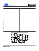
2. PIN DESCRIPTION
Clock Generator
Crystal Out
Crystal In
1,24
XOUT, XIN – The output and input of an inverting amplifier. Oscillation occurs when connected to
a crystal, providing an on-chip system clock. Alternatively, an external clo ck can be supplied to
the XIN pin to provide the system clock for the device.
CPU Clock Output 2
CPUCLK – Output of on-chip oscillator which can drive one standard CMOS load.
Control Pins and Serial Data I/O
Serial Clock Input 5
SCLK – A Schmitt-trigger input pin. Clocks data from the SDI pin into the receive buffer and out
of the transmit buffer onto the SDO pin when CS
is low.
Serial Data Output 6
SDO – Serial port data output pin.SDO is forced into a high-impedance state when CS is high.
Chip Select 7
CS – Low, activates the serial port interface.
Mode Select 8
MODE - High, enables the “auto-boot” mode. The mode pin has an internal pull-down resistor.
Energy Output 18,21,22
E3, E1, E2 – Active-low pulses with an output frequency proportional to the selected power . Con-
figurable outputs for active, app arent, and reactive power, negative energy indication, zero cross
detection, and power failure monitoring. E1
, E2, E3 outputs are configured in the Operational
Modes Register.
Reset 19
RESET – A Schmitt-trigger input pin. Low activates Reset, all internal registers (some of which
drive output pins) are set to their default states.
Interrupt 20
INT - Low, indicates that an enabled event has occurred.
Serial Data Input 23
SDI - Serial port data input pin. Data will be input at a rate determined by SCLK.
Analog Inputs/Outputs
Differential Voltage Inputs 9,10
VIN+, VIN- – Differential analog input pins for the voltage channel.
Differential Current Inputs 15,16
IIN+, IIN- – Differential analog input pins for the current channel.
Voltage Reference Output 11
VREFOUT – The on-chip voltage reference output. The voltage reference has a nominal magni-
tude of 2.5 V and is referenced to the AGND pin on the converter.
Voltage Reference Input 12
VREFIN – The input to this pin establishes the voltage reference for the on-chip modulator.
Power Supply Connections
Positive Digital Supply 3
VD+ – The positive digital supply.
Digital Ground 4
DGND – Digital Ground.
Positive Analog Supply 14
VA+ – The positive analog supply.
Analog Ground 13
AGND – Analog ground.
Power Fail Monitor
17
PFMON – The power fail monitor pin monitors the analog supply. If the analog supply does not
meet or falls below PFMON’s voltage threshold, a Low-supply Detect (LSD) event is set in the
status register.
12
11
10
9
8
7
6
5
4
3
2
1
13
14
15
16
17
18
19
20
21
22
23
24
AGND Analog Ground
VA+ Positive Analog Supply
IIN - Differential Cu rrent Input
IIN + Differential Cu rrent Input
PFMON Power Fa il Mo nitor
E3 High Frequency Energy Output
RESET Reset
INT In terrup t
E1 Energy Output 1
SDI Se rial D ata Input
XIN Cr ysta l In
E2
Energy Output 2
VREFINVoltage Reference Input
VREFOUTVoltage Reference Output
VIN-Differential Voltage Input
VIN+Differential Voltage Input
MODEMode Select
CSChip Select
SDOSerial Data Ouput
SCLKSerial C lock
DGNDDigital Ground
VD+Positive Digita l Supp ly
CPUCLKCPU Clock Output
XOUTCrystal Out