
User Manual


CS5463
18 DS678F3
The pulse output frequency of E1 is directly proportional
to the active power calculated from the input signals. To
calculate the output frequency of E1
, the following trans-
fer function can be utilized:
With MCLK = 4.096 MHz, PF = 1, and default settings,
the pulses will have an average frequency equal to the
frequency specified by
PulseRate when the input sig-
nals applied to the voltage and current channels cause
full-scale readings in the instantaneous voltage and cur-
rent registers. The maximum pulse frequency from the
E1
pin is (MCLK/K)/2048.
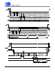
5.5.2 Apparent Energy Mode
Pin E2 outputs apparent ener gy pulses when th e Oper-
ational Mode Register
bit E2MODE = 1. Pin E3 ou tput s
apparent energy pulses when the
Operational Mode
Register
bits E3MODE[1:0] = 3 (11b). Figure 6 illus-
trates the pulse output format with apparent energy on
E2
(E2MODE = 1 and E3MODE[1:0 ] = 0)
The pulse output freque ncy of E2
(and/or E3) is directly
proportional to the apparent power calculated from the
input signals. Since apparent power is without reference
to an impedance phase angle, the following transfer
function can be utilized to calculate the output frequency
on E2
(and/or E3).
With MCLK = 4.096 MHz and default settings, the puls-
es will have an average frequency equal to the frequen-
cy specified by
PulseRate when the input signals
applied to the voltage and current channels cause
full-scale readings in the instantaneous voltage and cur-
rent registers. The maximum pulse frequency from the
E2
(and/or E3) pin is (MCLK / K) /2048. The E2 (and/or
E3
) pin outputs apparent energy, but has no energy di-
rection indicator.
5.5.3 Reactive Energy Mode
Reactive energy pulses are output on pin E3 by setting
bit E3MODE[1:0] = 0 (def ault) in the
Operational Mode
Register
. Positive reactive energy is registered by E3
falling when E2 is high. Negative reactive energy is reg-
istered by E3
falling when E2 is low. Figure 5 on
page 17 illustrates the pulse output format with negative
reactive energy o utput on pin E3
and the sign of the en-
ergy on E2
. The E3 and E2 pulse output switching char-
acteristics are specified in Figure 2 on page 13.
The pulse output frequency of E3
is directly propor tional
to the reac tive power calcula ted from the in put signals.
To calculate the output frequency on E3
, the following
transfer function can be utilized:
With MCLK = 4.096 MHz, PF = 0 and default settings,
the pulses will have an average frequency equal to the
frequency specified by
PulseRate when the input sig-
nals applied to the voltage and current channels cause
full-scale readings in the instantaneous voltage and cur-
rent registers. The maximum pulse frequency from the
E1
pin is (MCLK/K)/2048.
5.5.4 Voltage Channel Sign Mode
Setting bits E3MODE[1:0] = 2 (10b) in the Operational
Mode Register
outputs the sign of the voltage channel
on pin E3
. Figure 7 illustrates the output format with volt-
age channel sign on E3
FREQ
P
= Average frequency of active energy E1 pulses [Hz]
VIN = rms voltage across VIN+ and VIN- [V]
VGAIN = Voltage channe l gain
IIN = rms voltage across IIN+ and IIN- [V]
IGAIN = Current channel gain
PF = Power Factor
PulseRate = PulseRateE x (MCLK/K)/2048 [Hz]
VREFIN = Voltage at VREFIN pin [V]
FREQ
P
VIN VGAIN IIN IGAIN PF PulseRate
VREFIN
2
---------------------------------------------------------------------------------------------------------------------------------=
E3
E2
E1
Figure 6. Apparent energy pulse out puts
FREQ
S
= Average frequency of apparent energy E2 and/or E3 pulses [Hz]
VIN = rms voltage across VIN+ and VIN- [V]
VGAIN = Voltage channe l gain
IIN = rms voltage across IIN+ and IIN- [V]
IGAIN = Current channel gain
PulseRate = PulseRateE x (MCLK/K)/2048 [Hz]
VREFIN = Voltage at VREFIN pin [V]
FREQ
S
VIN VGAIN IIN IGAIN PulseRate
VREFIN
2
------------------------------------------------------------------------------------------------------------------=
FREQ
Q
= Average frequency of reactive energy E3 pulses [Hz]
VIN = rms voltage across VIN+ and VIN- [V]
VGAIN = Voltage channe l gain
IIN = rms voltage across IIN+ and IIN- [V]
IGAIN = Current channel gain
PQ =
PulseRate = PulseRateE x (MCLK/K)/2048 [Hz]
VREFIN = Voltage at VREFIN pin [V]
FREQ
Q
VIN VGAIN IIN IGAIN PQ PulseRate
VREFIN
2
----------------------------------------------------------------------------------------------------------------------------------=
1PF
2
–
E3
E2
E1
Figure 7. Voltage Channel Sign Pulse outputs