
User Manual


CS5463
DS678F3 17
for unsigned re gisters is a n ormalized value betw een 0
and 1. A register value of
represents the maximum possible value.
At each instantaneous measurement, the CRDY bit will
be set in the
Status Register, and the INT pin will be-
come active if the CRDY bit is unmasked in the
Mask
Register
. At the end of each computation cycle, the
DRDY bit will be set in the
Status Register, and the INT
pin will become active if the DRDY bit is unmasked in
the
Mask Register . When these bits are asserted, they
must be cleared before they can be asserted again.
If the
Cycle Count Register (N) is set to 1, all output cal-
culations are instantaneous, and DRDY, like CRDY, will
indicate when instantaneous measurements are fin-
ished. Some calculations are inhibited when the cycle
count is less than 2.
Epsilon (
) is the ratio of the input line frequency (f
i
) to
the sample frequency (f
s
) of the ADC.
where f
s
= MCLK / (K*1024). With MCLK = 4.096 MHz
and clock divider K = 1, f
s
= 4000 Hz. For the two
most-common line frequencies, 50 Hz and 60 Hz
and
respectively. Epsilon is used to set the frequency of the
internal sine/cosine reference for the fundamental ac-
tive and reactive measureme nts, and the gain of the 90°
phase shift (IIR) filter for the average reactive power.
5.5 Energy Pulse Output
The CS5463 provides three output pins for energy reg-
istration. By default, E1
registers active energy, E3 reg-
isters reactive energy, and E2
indicates the sign of both
active and reactive energy. (See Figure 2.
Timing Dia-
gram for E1, E2, and E3
on page13.) T he E1 pulse out-
put is designed to register the Active Energy. The E2
pin
can be set to register Ap parent Energy. Table 2 defines
the pulse output mode, which is controlled by bit
E2MODE in the
Operational Mode Register .
The E3 pin can be set to register Reactive Energy (de-
fault), PFMON, Voltage Channel Sign, or Apparent En-
ergy. Table 3 defines the pulse output format, which is
controlled by bits E3MODE[1:0] in the
Operational
Mode Register.
The pulse output frequency o f E1, E2, and E3 is directly
proportional to the power calculated from the input sig-
nals. The value contained in the
PulseRateE Register is
the ratio of the frequency of energy-outpu t pulses to the
number of sample s, at full scale, which defines th e av-
erage frequency for th e ou tp ut pulses. The pulse width,
t
pw
in Figure 2, is programmable through the Pulse-
Width register, and is approximately equal to:
If MCLK =
4.096 MHz, K = 1, and PulseWidth = 1, then
t
pw
0.25 ms.
5.5.1 Active Energy
The E1 pin produces active-low pulses with an output
frequency proportional to the active power. The E2
pin
is the energy direction indicator. Positive energy is rep-
resented by E1
pin falling while the E2 is high. Negative
energy is represented by the E1
pin falling while the E2
is low. The E1 and E2 switching characteristics are
specified in Figure 2.
Timing Diagram for E1, E2, and E3
on page13.
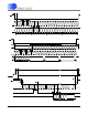
Figure 5 illustrates the pulse output format with positive
active energy and negative re active energy.
2
23
1–
2
23
------------------------
0.99999988
=
f
i
f
s
=
50 Hz 4000 Hz 0.0125==
60 Hz 4000 Hz 0.015==
E2MODE E2 Output Mode
0 Sign of Energy
1 Apparent Energy
Table 2. E2 Pin Configuration
E3MODE1 E3MODE0 E3
OutPut Mode
0 0 Reactive Energy
01 PFMON
1 0 Voltag e Channel Sign
1 1 Apparent Energy
Table 3. E3 Pin Configuration
t
pw
secPulseWidth
1
( MCLK/K ) / 1024
------------------------------------------------
E3
E2
E1
Figure 5. Active and Reactive energy pulse outputs