
User Manual


CS5463
14 DS678F3
4. THEORY OF OPERATION
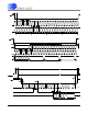
The CS5463 is a dual-channel analog-to-digital convert-
er (ADC) followed by a computation engine that per-
forms power calculations and energy-to-pulse
conversion. The data flow for the voltage and current
channel measurement and the power calculation algo-
rithms are depic te d in Fig ur e 3 and 4, respe ctively.
The analog inputs are structured with two dedicated
channels,
Voltage and Current, then optimized to simpli-
fy interfacing to various sensing elements.
The voltage-sensing element introduces a voltage
waveform on the voltage channe l input VIN± and is sub-
ject to a gain of 10x. A second-order d elta-sigma mo du-
lator samples the amplified sig nal for digitization.
Simultaneously, the current-sensing element introduces
a voltage waveform on the current channel input IIN±
and is subject to two selectable gains of the program-
mable gain amplifier (PGA). The amplified signal is
sampled by a fourth-order delta-sigma modulator for
digitization. Both converters sample at a rate of
MCLK/8, the over-sampling provides a wide dynamic
range and simplified anti-alias filter design.
4.1 Digital Filters
The decimating dig ital filters on both chann els are Sinc
3
filters followed by 4th-order IIR filters. The single-bit
data is passed to the low-pass decimat ion filter and out-
put at a fixed word rate. The ou tput word is passed to an
optional IIR filter to compensate for the magnitude roll
off of the low-pass filtering operation.
An optional digital high-pass filter (
HPF in Figure 3) re-
moves any DC component from the selected signal
path. By removing the DC component from the voltage
and/or the current channel, any DC content will also be
removed from the calcu lated active power as we ll. With
both HPFs enabled the DC component will be removed
from the calculated V
RMS
and I
RMS
as well as the appar-
ent power.
When the optional HPF in either channel is disabled, an
all-pass filter (APF) is implemented. The APF has an
amplitude response that is flat within the channel ba nd-
width and is used for matching phase in syste ms where
only one HPF is engaged.
4.2 Voltage and Current Measurements
The digital filter output word is then subject to a DC off-
set adjustment and a gain calibration (See Section 7.
System Calibration on page 37). The calibrated mea-
surement is available by reading the instantaneous volt-
age and current registers.
The Root Mean Square (
RMS in Figure 4) calculations
are performed on N instantaneous voltage and current
samples, V
n and In, respectively (where N is the cycle
count), using the formula:
and likewise for V
RMS
, using Vn. I
RMS
and V
RMS
are ac-
cessible by register reads, which are updated once ev-
ery cycle count (referred to as a computational cycle).
4.3 Power Measurements
The instantaneous voltage and current samples are
multiplied to obtain the instantaneous power (see Fig-
ure 3). The product is then averaged over N conver-
sions to compute active power and is used to drive
energy pulse output E1
. Energy output E2 is selectable,
providing an energy sign or a pulse output that is pro-
portional to the apparent power. Energy output E3
VOLTAGE
SINC
3
+
X
V*
gn
CURRENT
SINC
3
+
X
I*
gn
DELAY
REG
DELAY
REG
I
DCoff
*
V
DCoff
*
PGA
+
+
Configuration Register *
Digital Filter
Digital Filter
HPF
2nd Order
Modulator
4th Order
Modulator
x10
X
X
SYS
Gain
*
PC6 PC5 PC4 PC3
PC2
PC1 PC0
6
*
DENOTES REGISTER NAME.
DELAY
REG
DELAY
REG
HPF
V
Q
*
XVDEL XIDEL
012
2322
87
...
Operational Modes Register *
+
X
+
X
X
Q
*
2
MUX
X
V
*
P
*
I
*
MUX
VHPF IHPF
65
*
APF
HPF
APF
MUX
IIR
MUX
IIR
3
IIR
4
Figure 3. Data Measureme nt Flow Diagram.
I
RMS
I
n
n0=
N1–
N
---------------------
=