
Manual

CS5462
DS547F1 9
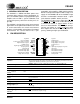
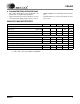
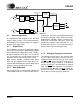
3.1 Theory of Operation
A computational flow diagram for the two data
paths is shown in Figure 1. The analog waveforms
at the voltage/current channel inputs are subject to
the gains of the input PGAs.
3.1.1 Digital Filters
The modulators convert the analog input voltages
on the I and V channels to a digital bitstream; which
is then filtered by the digital filter section. The digi-
tal filter is composed of low pass sinc
3
and IIR fil-
ters. The IIR filters are used to compensate for the
magnitude roll-off of the low pass filter section.
Both channels provide a high-pass filter option
which can be engaged into the signal path to re-
move the DC content from the current/voltage signal
before the energy calculations are made.
3.1.2 Gain Calibration
After being filtered, the instantaneous voltage and
current digital codes are used to calculate real av-
erage power. This power is then adjusted based on
the internal calibration setting defined at startup.
Calibrating the CS5462 is done by externally con-
necting the configuration input pins, CAL1 and
CAL0, to the program select output pins, P1 - P7,
in a particular sequence. These connections will in-
ternally compensate for small gain errors.
3.1.3 Energy-to-Frequency Conversion
The calibrated energy value is then converted into
a pulse output stream with a average frequency
proportional to the measured energy. Pulse output
pins E1
and E2 can be set to lower frequencies to
directly drive a stepper motor or a mechanical
counter or interface a microcontroller or infrared
LED. The FOUT
pulse output pin is set to max fre-
quency of 10 kHz. With full scale inputs on both the
current and voltage channels FOUT
will output
pulses with an average frequency of 10 kHz.
x
VIN±
IIN±
PGA Gain Select
HPF Select
Freq Select
Energy to
Pulse Rate
Converter
E1
E2
FOUT
Calibration
Digital
Filters
Digital
Filters
4
th
Order
Modulator
2
nd
Order
Modulator
PGA
10x
x
On-Chip
Configuration
Output Mode Select
HPF
HPF
Figure 1. Data Flow