
Instruction Manual
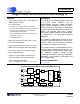

CS5461A
DS661F3 9
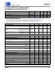
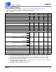
DIGITAL CHARACTERISTICS
• Min / Max characteristics and specifications are guaranteed over all Recommended Operating Conditions.
• Typical characteristics and specifications are measured at nominal supply voltages and TA = 25 °C.
• VA+ = VD+ = 5V ±5%; AGND = DGND = 0 V. All voltages with respect to 0 V.
• MCLK = 4.096 MHz.
Notes: 9. All measurements performed under static conditions.
10. If a crystal is used, then XIN frequency must remain between 2.5 MHz - 5.0 MHz. If an external oscillator is used,
XIN frequency range is 2.5 MHz - 20 MHz, but K must be set so that MCLK is between 2.5 MHz - 5.0 MHz.
11. If external MCLK is used, then the duty cycle must be between 45% and 55% to maintain this specification.
12. The frequency of CPUCLK is equal to MCLK.
13. The minimum FSCR is limited by the maximum allowed gain register value. The maximum FSCR is limited by the
full-scale signal applied to the channel input.
14. Configuration Register bits PC[6:0] are set to “0000000”.
15. The MODE pin is pulled low by an internal resistor.
Parameter Symbol Min Typ Max Unit
Master Clock Characteristics
Master Clock Frequency Internal Gate Oscillator (Note 10) MCLK 2.5 4.096 20 MHz
Master Clock Duty Cycle 40 - 60 %
CPUCLK Duty Cycle (Note 11 and 12) 40 60 %
Filter Characteristics
Phase Compensation Range (Voltage Channel, 60 Hz) -2.8 - +2.8 °
Input Sampling Rate DCLK = MCLK/K - DCLK/8 - Hz
Digital Filter Output Word Rate (Both Channels) OWR - DCLK/1024 - Hz
High-pass Filter Corner Frequency -3 dB - 0.5 - Hz
Full Scale Calibration Range (
Referred to Input) (Note 13) FSCR 25 - 100 %F.S.
Channel-to-channel Time-shift Error (Note 14) 1.0 µs
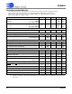
Input/Output Characteristics
High-level Input Voltage
All Pins Except XIN and SCLK and RESET
XIN
SCLK and RESET
V
IH
0.6 VD+
(VD+) - 0.5
0.8VD+
-
-
-
-
-
-
V
V
V
Low-level Input Voltage (VD = 5 V)
All Pins Except XIN and SCLK and RESET
XIN
SCLK and RESET
V
IL
-
-
-
-
-
-
0.8
1.5
0.2VD+
V
V
V
Low-level Input Voltage (VD = 3.3 V)
All Pins Except XIN and SCLK and RESET
XIN
SCLK and RESET
V
IL
-
-
-
-
-
-
0.48
0.3
0.2VD+
V
V
V
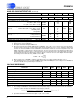
High-level Output Voltage I
out
= +5 mA V
OH
(VD+) - 1.0 - - V
Low-level Output Voltage I
out
= -5 mA V
OL
--0.4V
Input Leakage Current (Note 15) I
in
-±1±10µA
3-state Leakage Current I
OZ
--±10µA
Digital Output Pin Capacitance C
out
-5-pF